Supercharge Your Innovation With Domain-Expert AI Agents!

IO channel debugging method and system between fpga chips

A debugging method and a debugging system technology, applied in the communication field, can solve the problems that the dynamic phase debugging mode cannot be directly applied to FPGA device IO debugging, and achieve the effects of enhancing stability, reducing dependence, and improving work efficiency

Active Publication Date: 2016-01-20
NEUSOFT CORP
View PDF3 Cites 0 Cited by
  • Summary
  • Abstract
  • Description
  • Claims
  • Application Information

AI Technical Summary

Problems solved by technology

[0005] This dynamic phase debugging mode cannot be directly applied to IO debugging with FPGA devices at both ends

Method used


Image

  • IO channel debugging method and system between fpga chips
  • IO channel debugging method and system between fpga chips
  • IO channel debugging method and system between fpga chips

Examples


Embodiment Construction

[0018] In the following, preferred embodiments of a method for debugging an IO channel between FPGA chips and a system for debugging an IO channel between FPGA chips related to the present invention will be described with reference to the accompanying drawings.

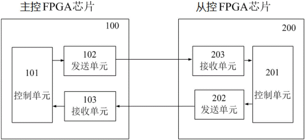
[0019] figure 1 It is a block diagram representing the general structure of the FPGA chip involved in the present invention; figure 2 It is a block diagram showing the connection relationship between the main control FPGA chip and the slave control FPGA chip involved in the present invention.

[0020] Such as figure 1 As shown, the FPGA chip 10 involved in the present invention includes a control unit 11, a sending unit 12 and a receiving unit 13, the sending unit 12 is used to send control signals and data to the outside, and the receiving unit 13 is used to receive external Control signals and data, etc., the control unit 11 is used to control the actions of the sending unit and the receiving unit.

[0021] refe...


PUM


Abstract

The invention provides a method and system for input-output (IO) channel debugging of field programmable gate array (FPGA) chips. The method comprises the steps of enabling a main control FPGA chip and an auxiliary control FPGA chip to respectively send first training sequences for signal sampling training to each other; enabling the main control FPGA chip to send a second training sequence to the auxiliary control FPGA chip after finishing signal sampling training; enabling the auxiliary control FPGA chip receiving the second training sequence to also send the second training sequence to the main control FPGA chip after finishing the signal sampling training and simultaneously enter a normal communication mode; and enabling the main control FPGA chip receiving the second training sequence to also enter a normal communication mode. By using a main control unit, an auxiliary control unit and the two training sequences, a dynamic phase adjustment method is applied to phase adaptive communication work with two ends not being fixed IO channels, stability of IO channel communication is improved, and adaptive adjustment on eye pattern interval changes caused by clock frequency, a printed circuit board (PCB) production process and FPGA internal placement and routing can be achieved.

Description

technical field [0001] The invention relates to the communication field, in particular to a debugging method and system for an IO channel between FPGA chips. Background technique [0002] With the rapid development of the Internet, the bandwidth of network system security products is increasing, and a single software platform can no longer meet the demand. More and more architectures are processed by software platforms and FPGA (Field-programmable gate array, field-programmable gate array) hardware platforms. High-speed network data is limited by the logic resources and IO interface resources of a single FPGA chip, and the solution of building a large-scale hardware platform with multiple FPGAs is gradually emerging. [0003] In the communication application of IO interconnection lines between multiple FPGA chips, the stability of the IO channel is the prerequisite for the correct operation of the system. The IO eye diagram interval of each FPGA chip will be affected by fac...

Claims


Application Information

Patent Timeline
Patent Type & Authority Patents(China)
IPC IPC(8): G06F11/26G06F13/16
Inventor 曲贺
Owner NEUSOFT CORP
Features
  • R&D
  • Intellectual Property
  • Life Sciences
  • Materials
  • Tech Scout
  • Unparalleled Data Quality
  • Higher Quality Content
  • 60% Fewer Hallucinations
Learn More