Method and device for biface chip tin soldering glue preparation

A chip and solder technology, applied in the field of chip solder glue preparation method and device, can solve the problems of uneven size of solder joints, waste of raw materials, low qualification rate, etc., achieve uniform size of solder joints, full utilization, improve production efficiency and The effect of pass rate

Active Publication Date: 2014-02-12
CARDMATIX
View PDF5 Cites 5 Cited by
  • Summary
  • Abstract
  • Description
  • Claims
  • Application Information

AI Technical Summary

Problems solved by technology

[0015] One of the technical problems to be solved by the present invention is to provide a method for preparing glue for chip soldering in view of the defects of uneven size of solder joints, waste of raw materials, low efficiency, and low pass rate when soldering chips in the prior art
[0016] The second technical problem to be solved by the present invention is to provide a chip soldering glue preparation device in view of the above-mentioned defects of uneven solder joint size, waste of raw materials, low efficiency, and low pass rate when soldering chips in the prior art

Method used


Image

  • Method and device for biface chip tin soldering glue preparation
  • Method and device for biface chip tin soldering glue preparation
  • Method and device for biface chip tin soldering glue preparation

Examples


Embodiment Construction

[0054] In order to have a clearer understanding of the technical features, purposes and effects of the present invention, the specific implementation manners of the present invention will now be described in detail with reference to the accompanying drawings.

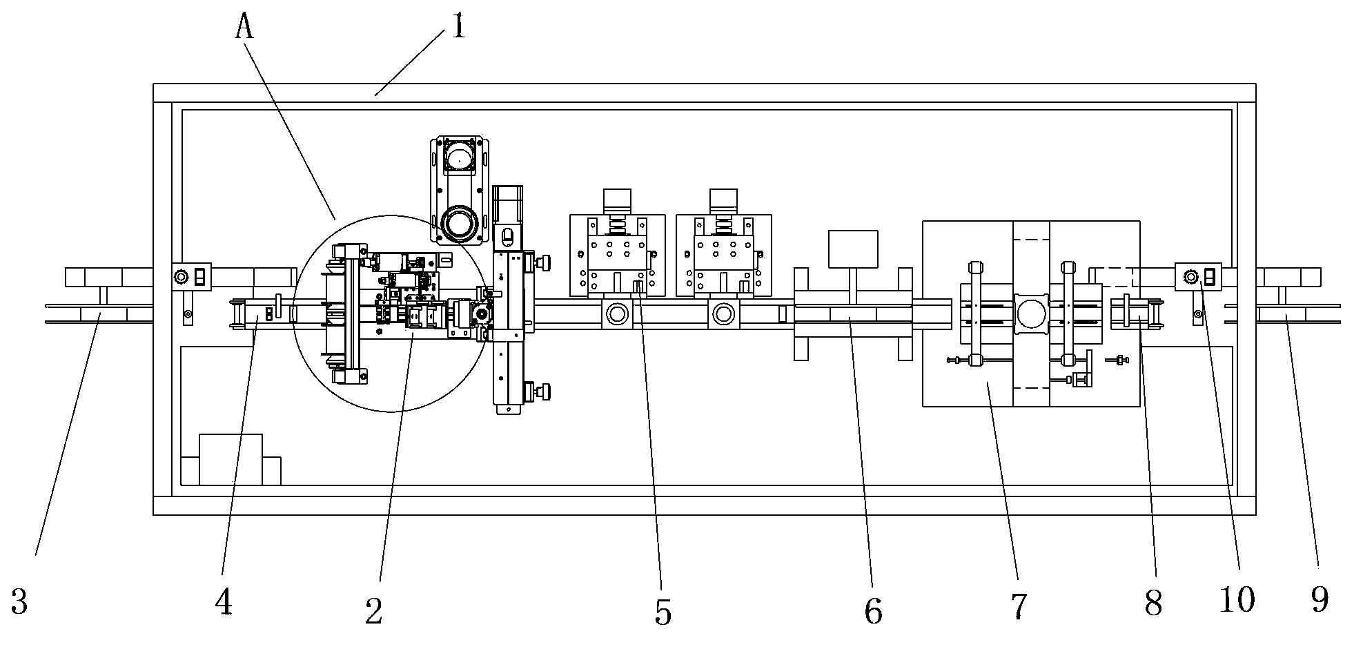
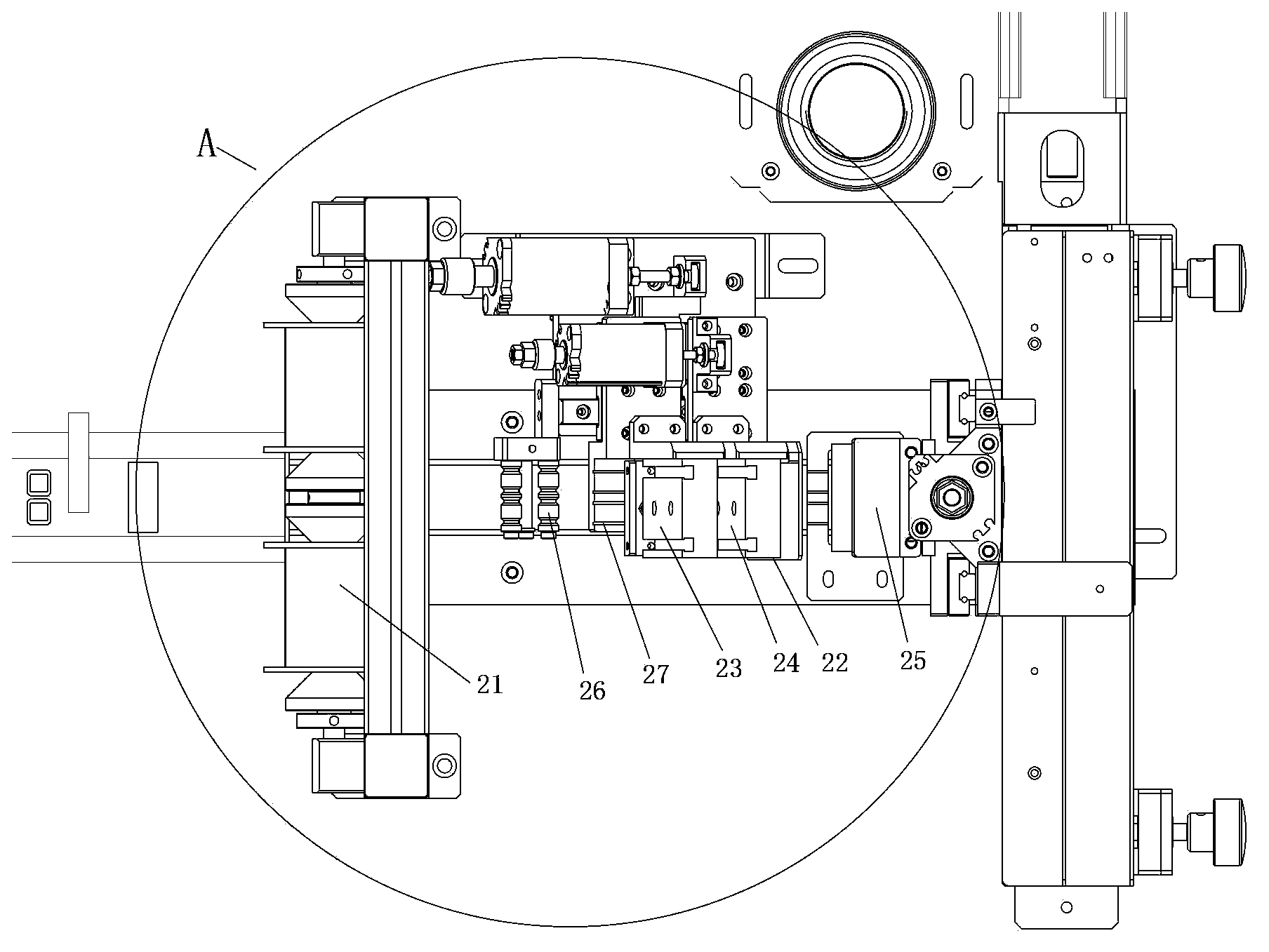
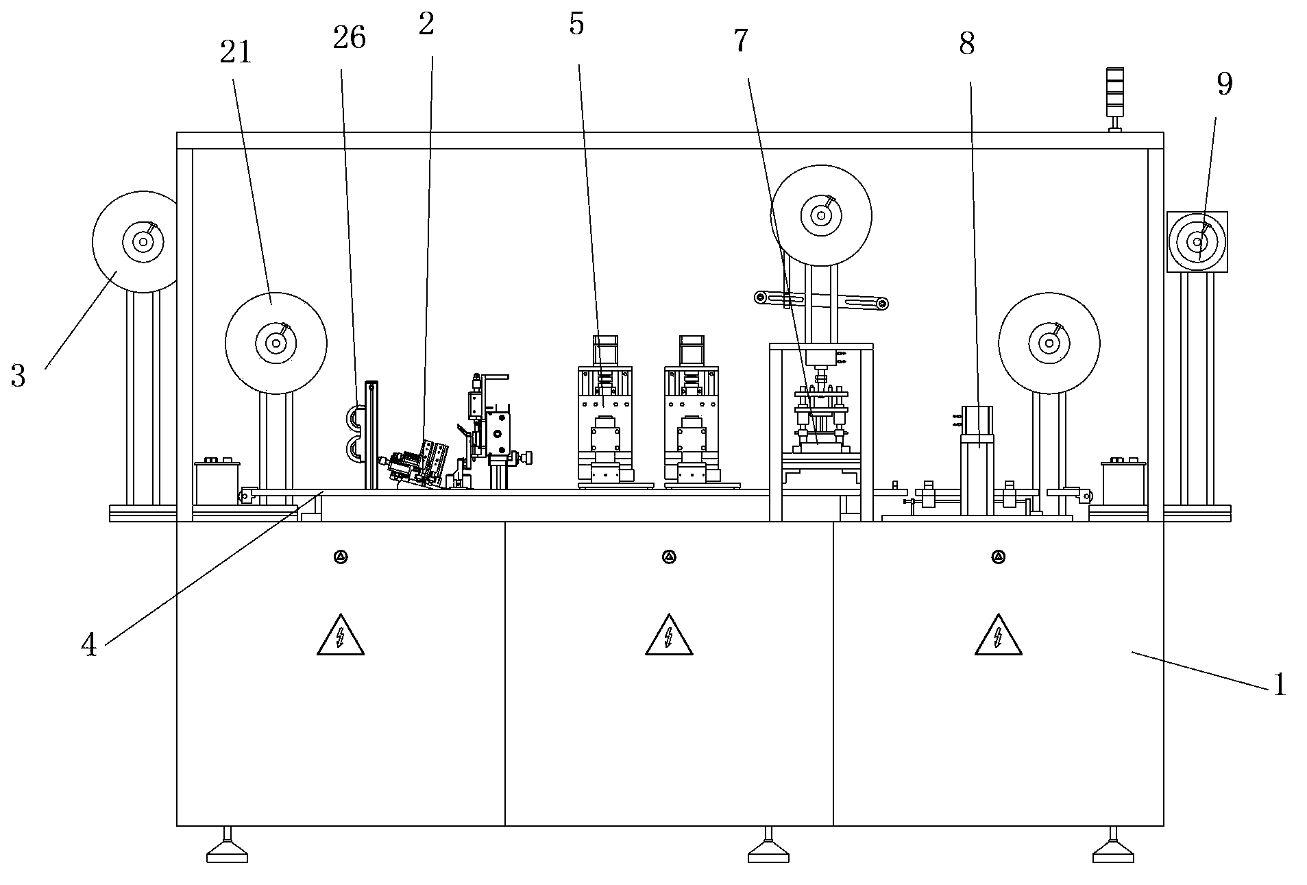
[0055] In the prior art, when the chip is soldered, the length of the tin wire sent to the predetermined soldering point of the chip is uneven, which often leads to defects such as uneven soldering point size, waste of raw materials, low efficiency, and low pass rate. The present invention aims at the above defects, The soldering method and device are restructured. The main technical means of the present invention are: first use the first crimping and feeding device to draw the tin wire, and then use the second crimping and feeding device to pull the tin wire to the predetermined soldering point of the chip, The moving distance of both pulling the tin wire is equal to the length of the tin wire required when soldering on...


PUM


Abstract

The invention discloses a method and device for biface chip tin soldering glue preparation. The method includes the steps first, tin is soldered on a predetermined solder joint of a chip; second, hot melt glue is soldered to the chip. In the first step, a tin wire is firstly pulled by a first wire pressing and feeding device, then, the tin wire is pulled to the predetermined solder joint of the chip through a second wire pressing and feeding device, both the moving distances of the tin wire pulled by the first wire pressing and feeding device and the second wire pressing and feeding device are equal to the length of the tin wire needed for tin soldering on the chip, and next tin soldering is performed on the predetermined solder joint by a tin soldering device. The device comprises a rack (1), a master control system arranged on the rack (1), and an automatic tin soldering set (2) which is arranged on the rack (1) and controlled by the master control system, the automatic tin soldering set (2) comprises a tin wire pay-off stand (21), a sliding way (22), the first wire pressing and feeding device (23), the second wire pressing and feeding device (24) and the tin soldering device (25). The method and device have the advantages that the length of the tin wire needed for tin soldering is accurate and controllable, and the production efficiency and the qualified rate are improved.

Description

technical field [0001] The invention relates to the field of mobile communication, and more specifically, to a chip soldering adhesive preparation method and a device thereof. Background technique [0002] With the rapid development of information technology and economy around the world, economic and information exchanges between people are becoming more and more frequent. Cards and contact CPU cards (smart cards) that are being used in many fields now. At present, smart cards still play an irreplaceable role in people's lives. Whether it is a contact smart card or a contactless smart card, it has its own advantages and disadvantages. The wear and tear between the contact smart card and the card machine greatly shortens its service life. . The application of non-contact cards is limited in the occasions where radio frequency interference is severe; secondly, due to the energy transfer through coupling, the power consumption is required to be very low; The technology and i...

Claims


Application Information

Patent Timeline
Patent Type & Authority Applications(China)
IPC IPC(8): H01L21/50H01L21/60G06K19/077
CPCG06K19/07743H01L24/11H01L24/81H01L2224/11H01L2224/75
Inventor 熊曙光
Owner CARDMATIX
Why Eureka
Try Eureka