Oxide TFT, manufacturing method of oxide TFT, display panel and display device

An oxide and substrate technology, applied in semiconductor/solid-state device manufacturing, transistors, electrical components, etc., can solve problems such as reducing the stability of display panels and affecting the overall performance of oxide TFTs, achieving stability assurance and improving stability. Effect

Inactive Publication Date: 2014-02-12
BEIJING BOE OPTOELECTRONCIS TECH CO LTD
View PDF8 Cites 25 Cited by
  • Summary
  • Abstract
  • Description
  • Claims
  • Application Information

AI Technical Summary

Problems solved by technology

This will seriously affect the overall performance of the...

Method used


Image

  • Oxide TFT, manufacturing method of oxide TFT, display panel and display device
  • Oxide TFT, manufacturing method of oxide TFT, display panel and display device
  • Oxide TFT, manufacturing method of oxide TFT, display panel and display device

Examples


no. 4 example

[0056] In order to avoid the occurrence of this situation, the present invention provides a further solution, i.e. the fourth embodiment, as follows:

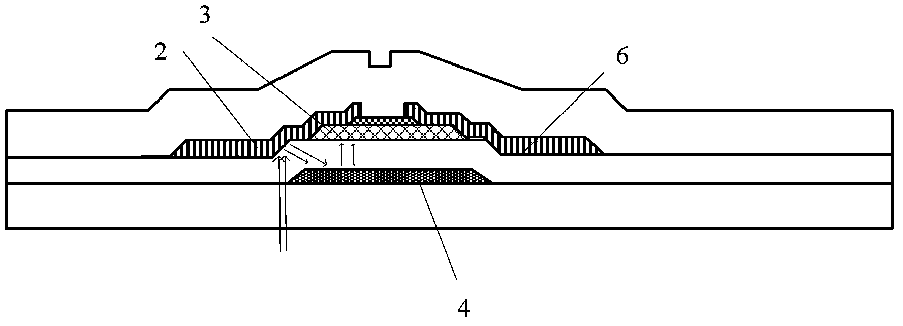
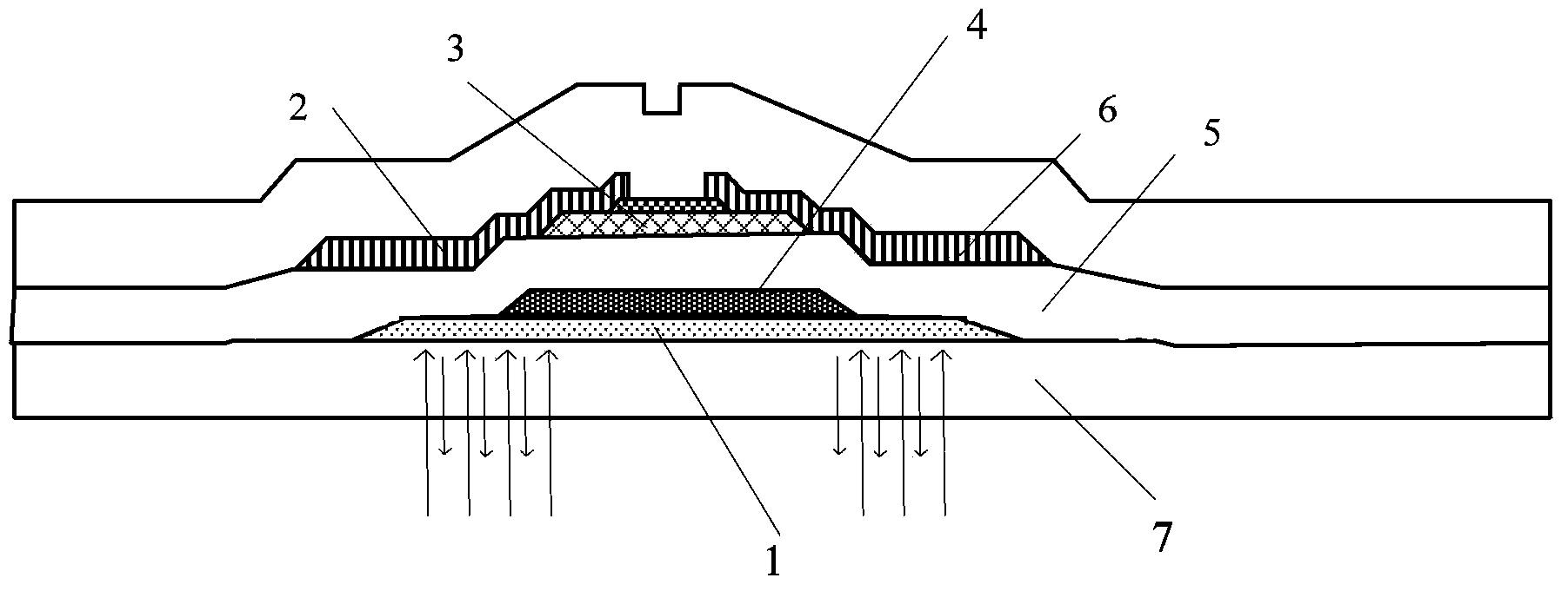
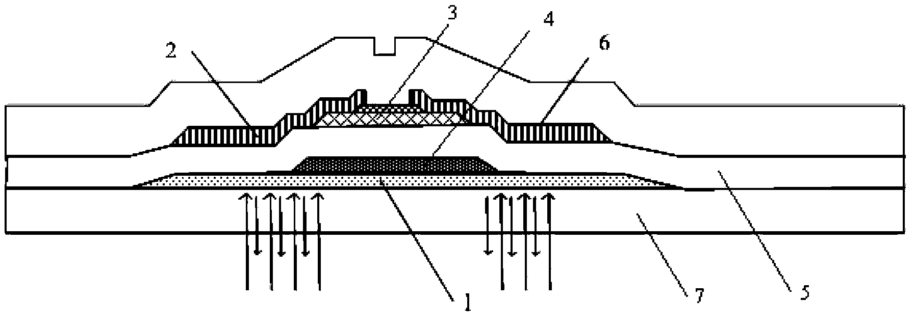
[0057] Such as Figure 5 As shown, the figure is a schematic structural diagram of the fourth embodiment of the oxide TFT of the present invention.

[0058] The difference between the fourth embodiment of the oxide TFT of the present invention and the third embodiment is that the pattern size of the light-shielding layer 1 may be greater than or equal to the pattern size of the source electrode 2 and the drain electrode 6 .

[0059] In this way, the light-shielding layer 1 of the oxide TFT of the fourth embodiment of the present invention can block all the light incident on the source 2 and the drain 6 from the back of the display panel, so as to prevent the light from entering the source 2 and the drain 6 from being transmitted through Multiple reflections incident to the oxide active layer 3 protect the oxide active layer 3 ...


PUM

PropertyMeasurementUnit
Thicknessaaaaaaaaaa
Thicknessaaaaaaaaaa

Abstract

The invention discloses an oxide TFT. The oxide TFT comprise a source electrode, a drain electrode, an oxide active layer, a grid insulating layer, a grid electrode and a shading layer, wherein the shading layer is formed on a substrate, the grid electrode is formed on the shading layer, the grid insulating layer covers the substrate where the grid electrode is formed, the oxide active layer is formed on the grid insulating layer, and the graphic size of the shading layer is larger than the graphic size of the grid electrode. The invention further discloses a manufacturing method of the oxide TFT, a corresponding display panel and a display device. According to the oxide TFT, the manufacturing method of the oxide TFT, the display panel and the display device, influence of the incident light on the back portion of the display panel on the property of the oxide TFT can be avoided, and stability of the oxide TFT is improved.

Description

technical field [0001] The invention relates to the technical field of liquid crystal display, in particular to an oxide thin film field effect transistor (Oxide TFT) and a preparation method thereof, a display panel and a display device. Background technique [0002] At present, oxide TFTs are mainly zinc oxide-based thin film field effect transistors, whose mobility is more than an order of magnitude higher than that of amorphous silicon transistors, and whose transparency to visible light is greater than 80%. It is one of the most promising next-generation thin film transistors. [0003] In the prior art, an important reason restricting the development of oxide TFT production is that metal oxide materials in oxide TFTs, such as indium gallium zinc oxide (IGZO), are not stable enough and are greatly affected by the outside world. External light irradiation will affect the electrical properties of metal oxides, resulting in an increase in leakage current. [0004] The exis...

Claims


Application Information

Patent Timeline
IPC IPC(8): H01L29/786H01L21/336
CPCH01L29/78633H01L27/1214H01L29/66742H01L29/7869
Inventor 李田生阎长江徐少颖谢振宇陈旭
Owner BEIJING BOE OPTOELECTRONCIS TECH CO LTD
Why Eureka
Try Eureka