Nitride semiconductor device

A nitride semiconductor, wiring layer technology, applied in the direction of semiconductor devices, semiconductor/solid-state device manufacturing, semiconductor/solid-state device components, etc., can solve the problems of increased on-resistance, inability to obtain, and inability to sufficiently reduce on-resistance , to achieve the effect of reducing wiring resistance, high maximum current, and increasing the number of wiring

Active Publication Date: 2014-02-12
PANASONIC INTELLECTUAL PROPERTY MANAGEMENT CO LTD
View PDF4 Cites 0 Cited by
  • Summary
  • Abstract
  • Description
  • Claims
  • Application Information

AI Technical Summary

Problems solved by technology

[0014] However, if the gate width of the FET is linearly extended, the on-resistance due to wiring resistance increases, and the on-resistance cannot be sufficiently reduced.
In addition, the voltage difference (ΔVGS) between the gate and the source decreases due to an increase in the source potential and a decrease in the gate potential, so that the maximum current expected by increasing the gate width cannot be obtained.

Method used


Image

  • Nitride semiconductor device
  • Nitride semiconductor device
  • Nitride semiconductor device

Examples


Embodiment approach

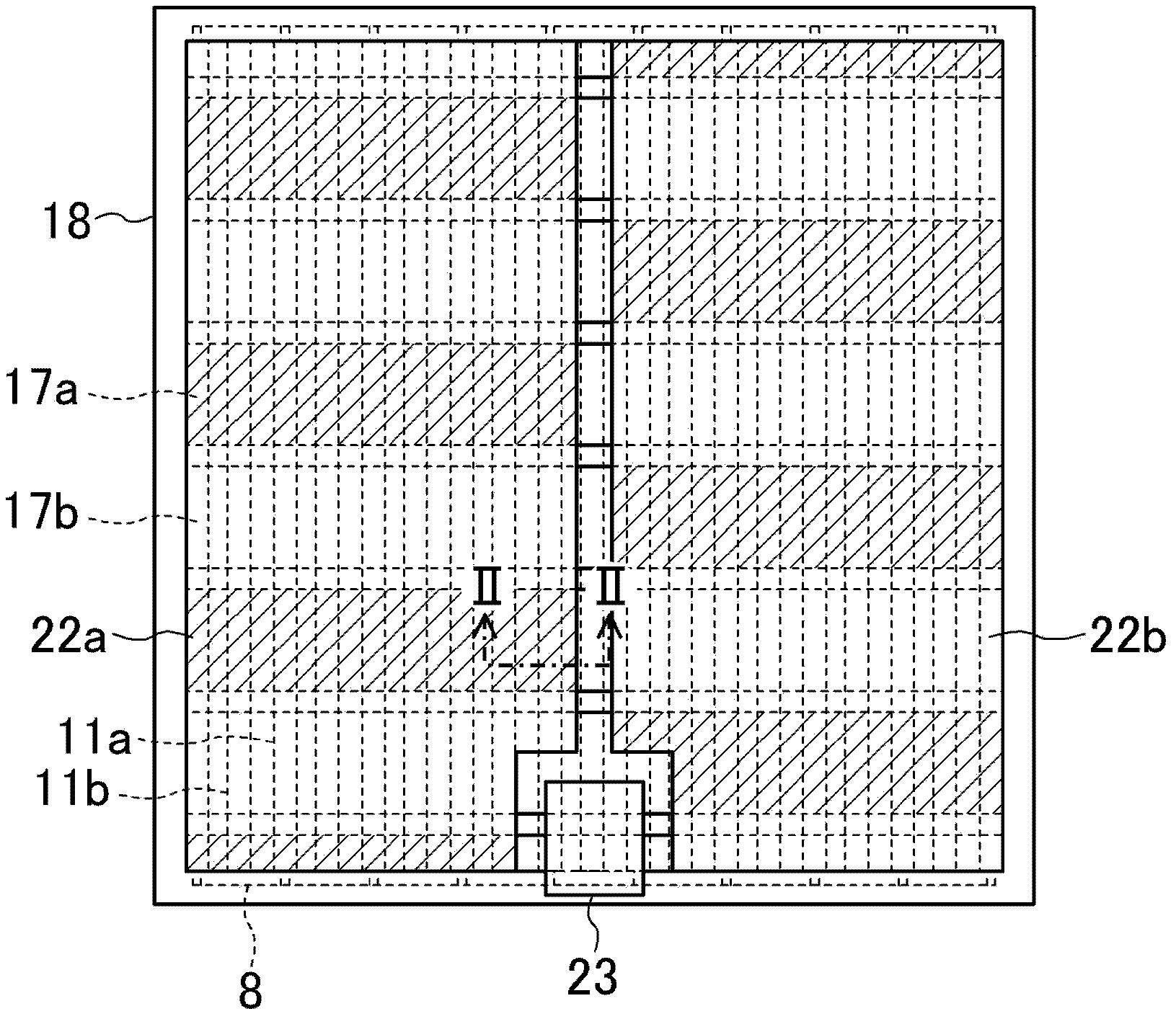
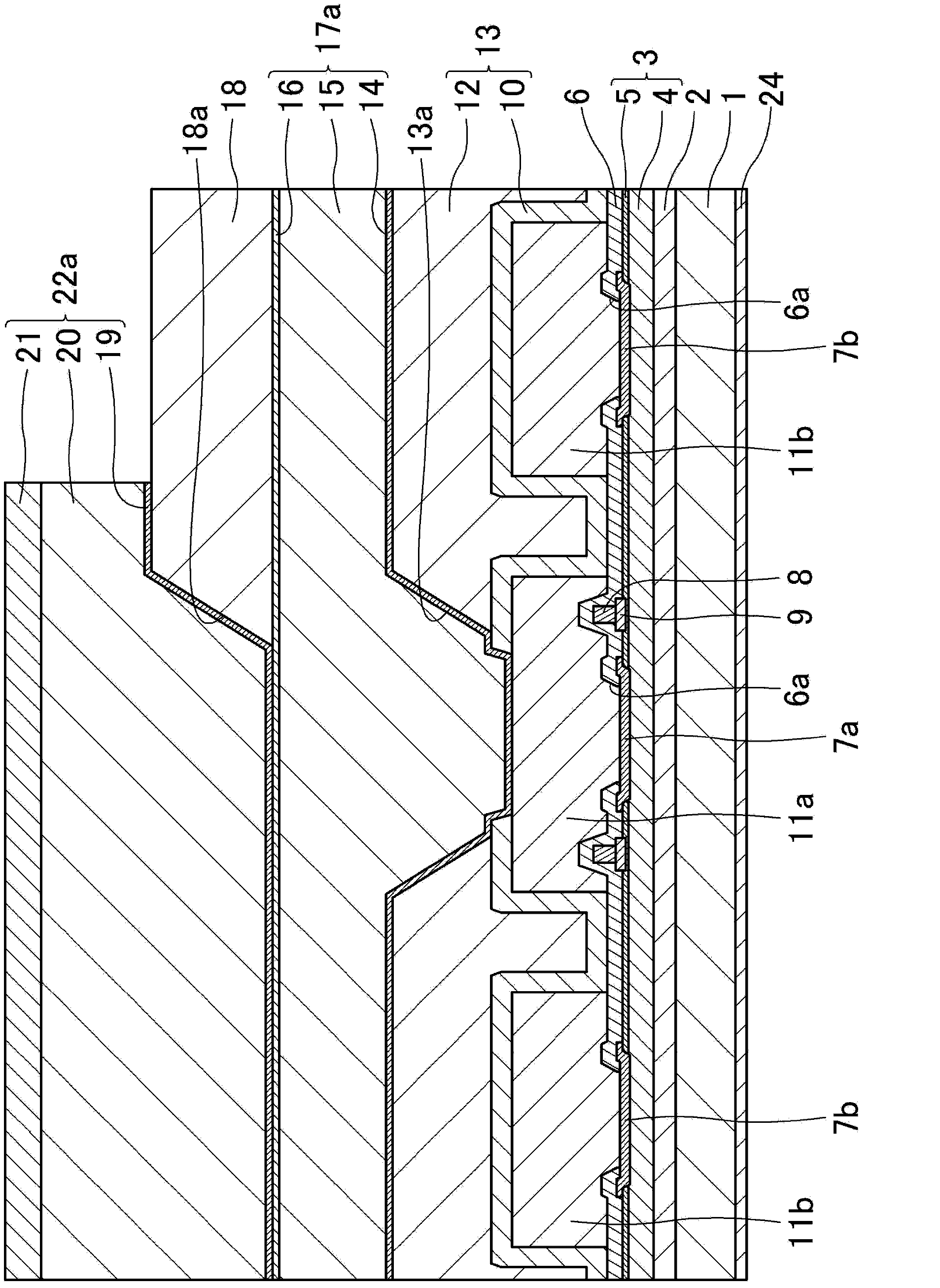
[0040] refer to Figure 1 ~ Figure 4 A nitride semiconductor device according to an embodiment of the present invention will be described.

[0041] like figure 1 as well as figure 2 As shown, in the nitride semiconductor device according to this embodiment, the buffer layer 2 and the nitride semiconductor layer 3 are sequentially formed on the substrate 1 made of silicon (Si). The nitride semiconductor layer 3 is composed of an undoped gallium nitride (GaN) layer 4 having a thickness of approximately 2.5 μm, and an undoped aluminum gallium nitride (AlGaN) layer 5 having a thickness of approximately 50 nm formed thereon. Two-dimensional electron gas (2DEG) is generated in the interface region between the undoped GaN layer 4 and the undoped AlGaN layer 5, and the 2DEG functions as a channel region.

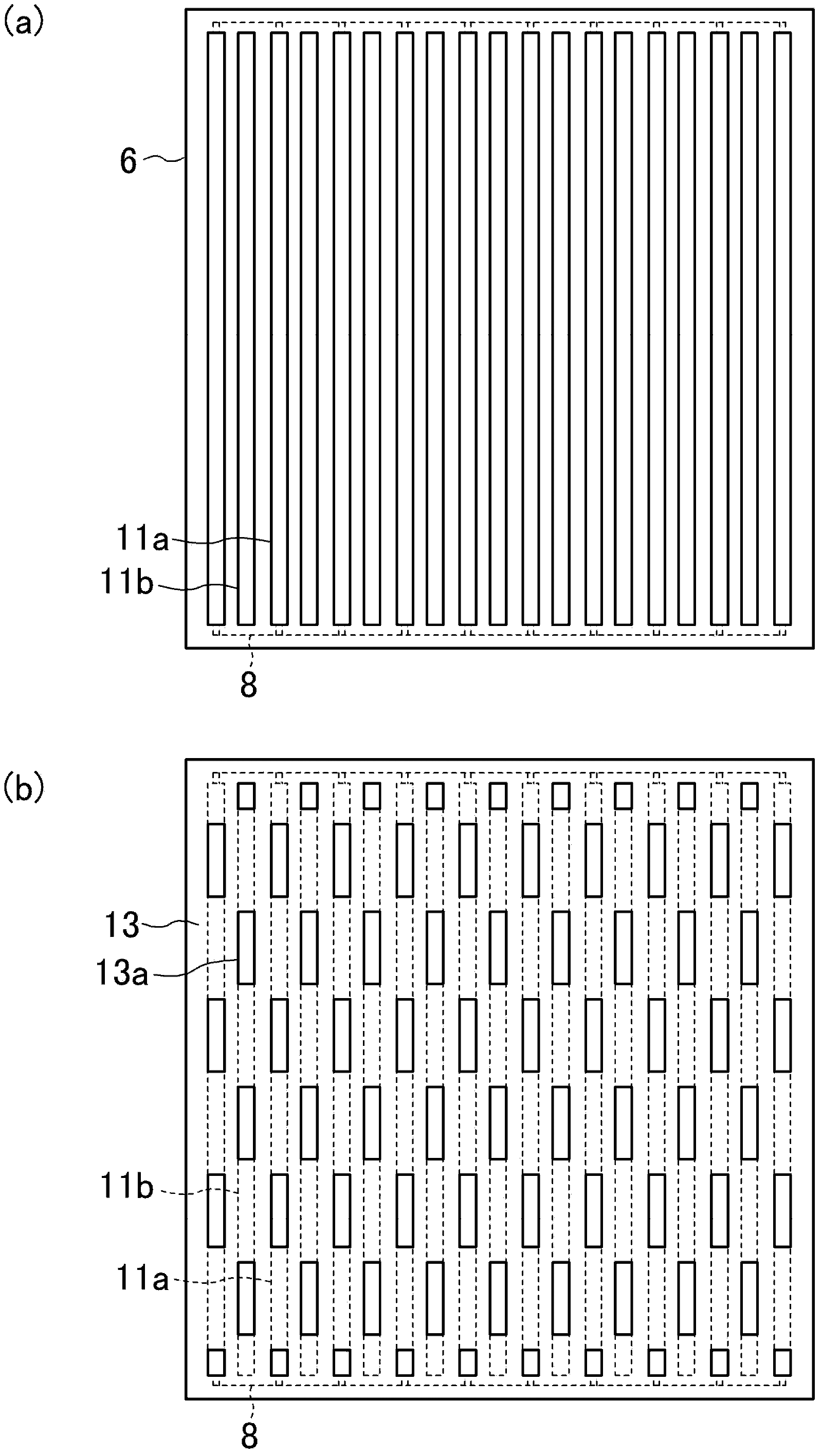
[0042] On the nitride semiconductor layer 3 , source electrodes 7 a as first electrodes and drain electrodes 7 b as second electrodes are separated from each other and alternate...


PUM


Abstract

A nitride semiconductor device is provided with: a first electrode wiring layer and a second electrode wiring layer, which are formed on a nitride semiconductor layer; a first insulating film, which is formed on the first electrode wiring layer and the second electrode wiring layer, and has first openings; a first wiring layer (17a) and a second wiring layer (17b), which are formed on the first insulating film, and are respectively connected to the first electrode wiring layer and the second electrode wiring layer via the first openings; a second insulating film (18), which is formed on the first wiring layer and the second wiring layer, and has second openings; and first pad layer (22a) and a second pad layer (22b), which are formed on the second insulating film, and are respectively connected to the first wiring layer and the second wiring layer via the second openings.

Description

technical field [0001] The nitride semiconductor device according to the present invention particularly relates to a nitride semiconductor device having an electrode pad formed on an active region. Background technique [0002] By the general formula AlxGal-x-yIn y N (where 0≤x≤1, 0≤y≤1, and 0≤x+y≤1) is a group III-V nitride semiconductor having a wide bandgap and a direct transfer type band structure as its physical characteristics , so it is applied to short-wavelength optical elements. Furthermore, since group III-V nitride semiconductors have characteristics of high breakdown electric field and high saturation electron velocity, their application to electronic devices and the like has been studied. [0003] In particular, the use of aluminum gallium nitride (AlGaN) grown epitaxially on a semi-insulating substrate x Ga 1-x N. Hetero-junction Field Effect Transistor (Hetero-junction Field Effect Transistor) of two-dimensional electron gas (2Dimensional Electron Gas: 2D...

Claims


Application Information

Patent Timeline
Patent Type & Authority Applications(China)
IPC IPC(8): H01L21/338H01L21/28H01L21/3205H01L21/768H01L23/522H01L29/41H01L29/417H01L29/778H01L29/812
CPCH01L24/37H01L2224/04034H01L24/06H01L2224/05639H01L2924/00014H01L23/4824H01L2224/37124H01L24/03H01L29/812H01L2224/05027H01L29/7787H01L24/05H01L23/482H01L2224/45124H01L2224/45014H01L2224/37144H01L29/2003H01L2224/45147H01L29/41725H01L2224/05644H01L2224/0345H01L24/45H01L2224/05611H01L2224/05671H01L2224/0346H01L24/00H01L23/53238H01L23/528H01L2224/04042H01L2224/06181H01L29/0692H01L2224/45144H01L2224/05655H01L2224/37147H01L2924/13062H01L2224/45015H01L2924/12032H01L2224/48639H01L2224/48644H01L2224/48655H01L2224/48671H01L2224/48811H01L2224/48839H01L2224/48844H01L2224/48855H01L2224/48871H01L2224/48611H01L2224/48711H01L2224/48739H01L2224/48744H01L2224/48755H01L2224/48771H01L29/1066H01L2924/00011H01L2924/13064H01L24/07H01L24/08H01L24/09H01L2224/0603H01L2924/00H01L2224/48H01L2924/01005H01L2224/84H01L2924/206H01L2224/73221
Inventor 海原一裕
Owner PANASONIC INTELLECTUAL PROPERTY MANAGEMENT CO LTD
Why Eureka
Try Eureka