Display device
A display device and display panel technology, which is applied in the direction of identification devices, static electricity, electrical components, etc., can solve problems such as inconvenience, achieve the effect of reducing assembly time and improving assembly convenience
- Summary
- Abstract
- Description
- Claims
- Application Information
AI Technical Summary
Problems solved by technology
Method used
Image
Examples
no. 1 approach
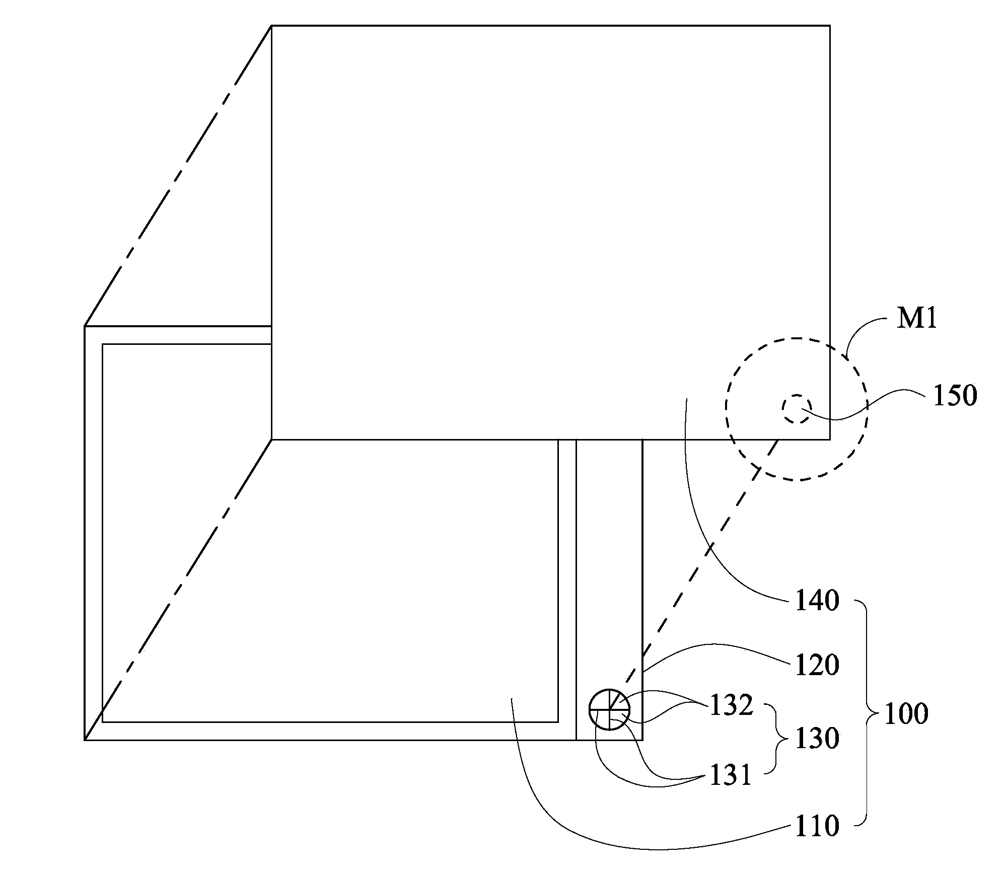
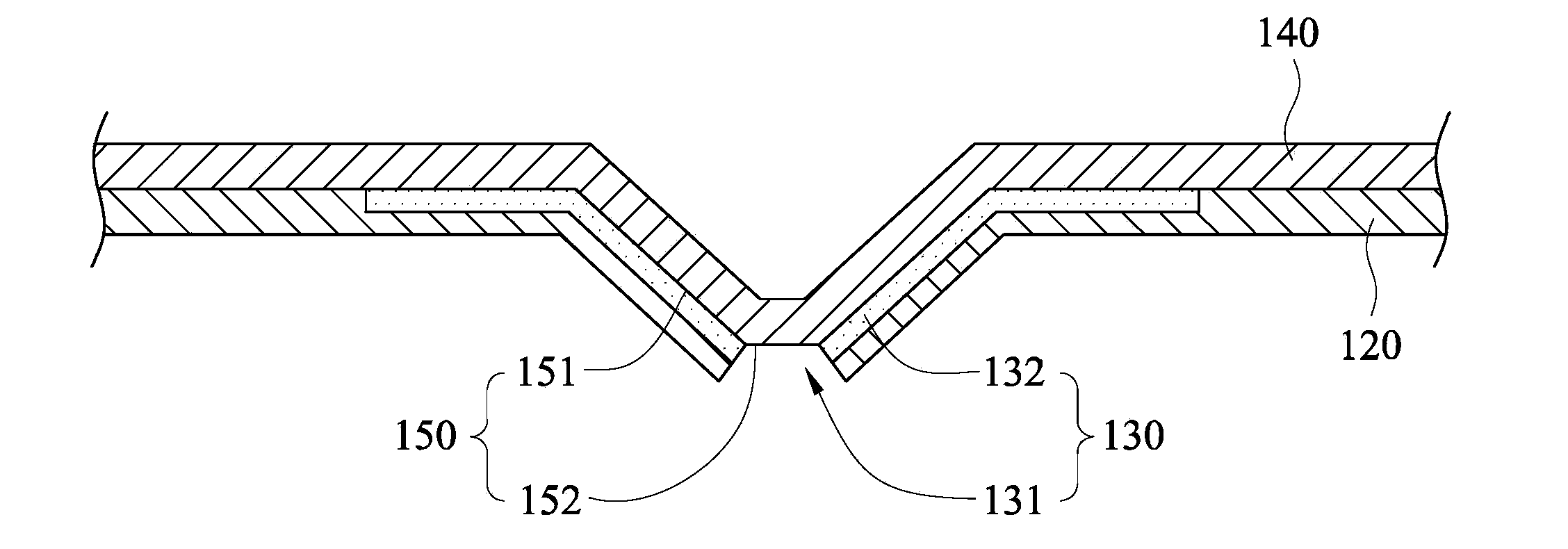
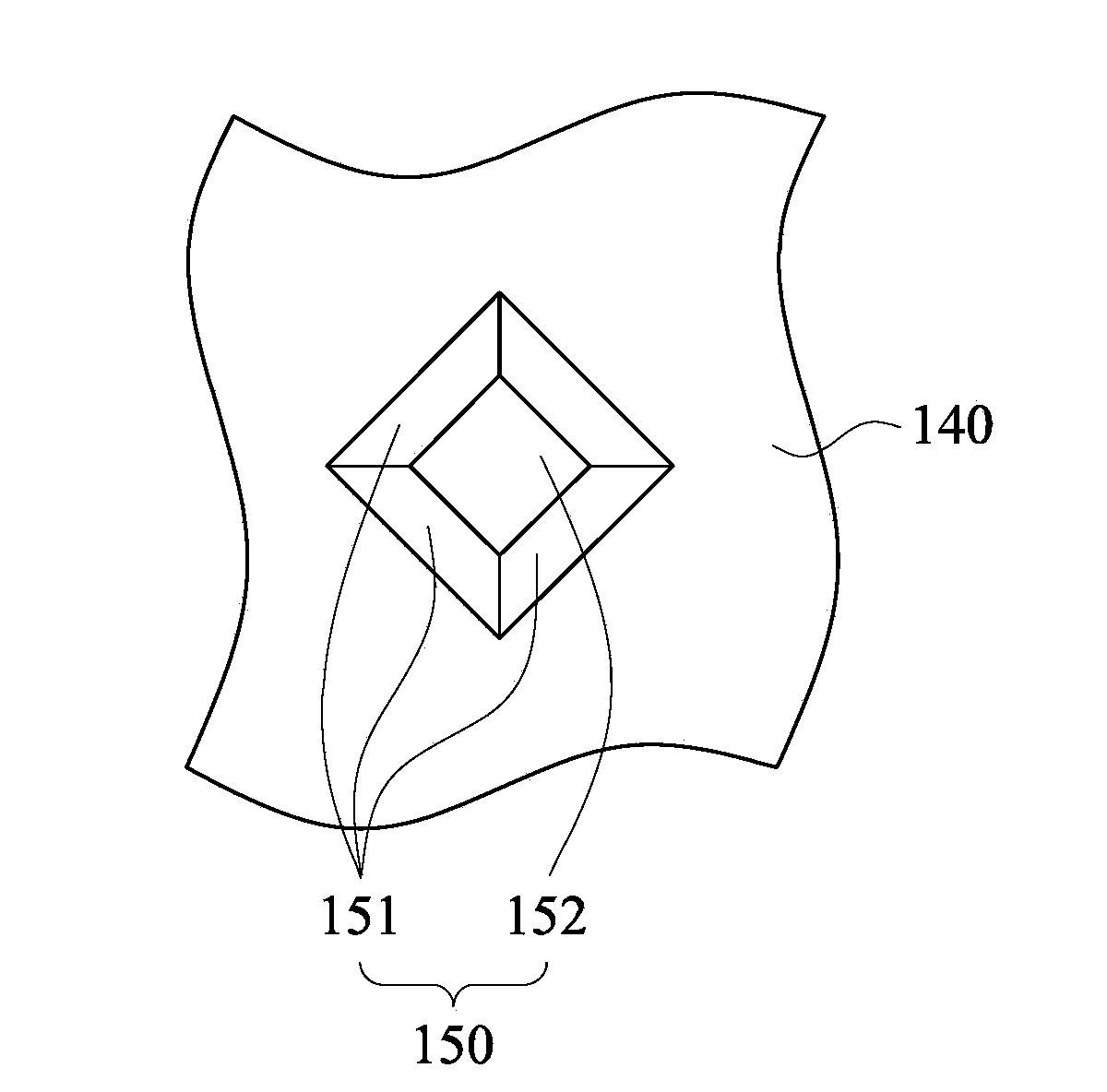
[0044] figure 1 An exploded view of the display device 100 according to the first embodiment of the present invention is shown. figure 2 draw figure 1 A partial cross-sectional view of the assembled part M1 of the display device 100 . Such as figure 1 and figure 2 , the display device 100 includes a display panel 110 , a circuit substrate 120 , a grounding pad 130 and a conductive shell 140 . The conductive shell 140 has a protruding portion 150 . The ground pad 130 is located on the circuit substrate 120 . The circuit substrate 120 is electrically connected to the display panel 110 . At least one cutting slit 131 is formed on the circuit substrate 120 and the ground pad 130 at the same time. The cutting slit 131 runs through the ground pad 130 and the circuit substrate 120 at the same time, and the cutting slit 131 defines a plurality of contact portions 132 on the ground pad 130 .
[0045] In this way, when the conductive shell 140 is assembled on the circuit board ...
no. 2 approach
[0053] Figure 4A A front view of the ground pad 230 according to the second embodiment of the present invention is shown. Figure 4B A front view of the protruding portion 250 according to the second embodiment of the present invention is shown. Such as Figure 4A and Figure 4B As shown, the display device of the second embodiment is substantially the same as the display device of the first embodiment, and the difference is that the pattern of the cutting slit 231 is in the shape of "one", that is, the number of the cutting slit 231 is only one. indivual. The cutting slit 231 is linearly formed on the ground pad 230 and the circuit substrate 120 , so that the number of contact portions 232 of the ground pad 230 is two (2*1). The number of contact surfaces 251 of the protruding portion 250 is two (2*1). In the second embodiment, the extreme protrusion 252 is a line edge, which is the intersection of the two contact surfaces 251 of the protrusion 250 . In this way, when ...
no. 3 approach
[0056] Figure 5A A front view of the ground pad 330 according to the third embodiment of the present invention is shown. Figure 5B A front view of the protruding portion 350 according to the third embodiment of the present invention is shown. Figure 5C draw Figure 5B side view. Such as Figure 5A and Figure 5B As shown, the display device of the third embodiment is substantially the same as the display device of the first embodiment, the difference is that the pattern of the cutting slit 331 is "X", that is, the number of the cutting slit 331 is 2, The number of contact portions 332 of the ground pad 330 is four (2*2). The protrusion 350 is a pyramid, for example, a four-sided pyramid, however, the present invention is not limited to the number of corners. The number of contact surfaces 351 of the protruding portion 350 is four (2*2). In the third embodiment, the extremely convex portion 352 is a pointed apex. The vertex is the intersection point of the four conta...
PUM
 Abstract
Description
Claims
Application Information


