

Multiple quantum well structure of high-brightness LED
A multi-quantum well structure and light-emitting diode technology, which is applied in the direction of electrical components, circuits, semiconductor devices, etc., can solve the problems of limited overall efficiency improvement potential, no overall consideration of stress release electron hole injection rate balance, etc., to achieve concentration distribution Improve compound position, increase compound efficiency, and improve overall performance
- Summary
- Abstract
- Description
- Claims
- Application Information
AI Technical Summary
Problems solved by technology
Method used
Image

Examples
Embodiment 1
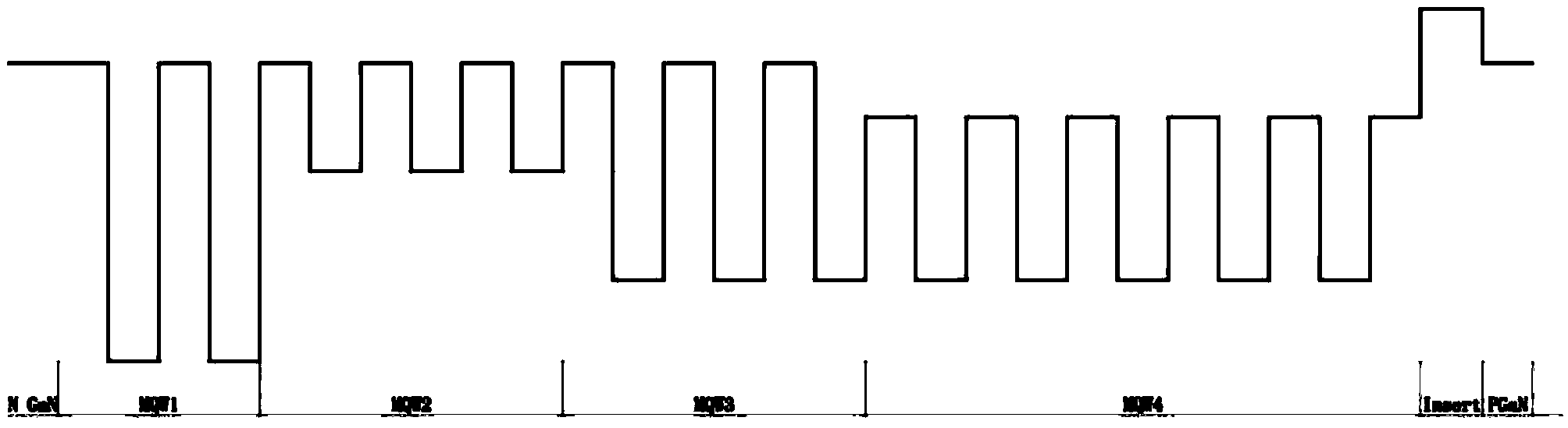
[0026] The multi-quantum well structure sequentially includes a first multi-quantum well layer, a second multi-quantum well layer, a third multi-quantum well layer and a fourth multi-quantum well layer. Wherein the first multi-quantum well layer is close to the side of the N-type layer, and the fourth multi-quantum well is close to the side of the P-type layer; the quantum well band gap of the first multi-quantum well layer is the smallest, and the quantum well of the second multi-quantum well layer is forbidden. The band width is the largest, the quantum well band gap of the third and the fourth multi-quantum well layer is between the quantum well band gap of the first multi-quantum well layer and the second multi-quantum well layer; the quantum barrier of the fourth multi-quantum well layer The bandgap width is smaller than the quantum barrier bandgap width of other multi-quantum well layers but larger than the quantum well bandgap width of the fourth quantum well layer; the ...
Embodiment 2
[0029] The multi-quantum well structure sequentially includes a first multi-quantum well layer, a second multi-quantum well layer, a third multi-quantum well layer and a fourth multi-quantum well layer. Wherein the first multi-quantum well layer is close to the side of the N-type layer, and the fourth multi-quantum well is close to the side of the P-type layer; the quantum well band gap of the first multi-quantum well layer is the smallest, and the quantum well of the second multi-quantum well layer is forbidden. The band width is the largest, the quantum well band gap of the third and the fourth multi-quantum well layer is between the quantum well band gap of the first multi-quantum well layer and the second multi-quantum well layer; the quantum barrier of the fourth multi-quantum well layer The band gap is smaller than the quantum barrier band gap of other multi-quantum well layers but larger than the quantum well band gap of the fourth quantum well layer; the number of layer...
Embodiment 3
[0032] The multi-quantum well structure sequentially includes a first multi-quantum well layer, a second multi-quantum well layer, a third multi-quantum well layer and a fourth multi-quantum well layer. Wherein the first multi-quantum well layer is close to the side of the N-type layer, and the fourth multi-quantum well is close to the side of the P-type layer; the quantum well band gap of the first multi-quantum well layer is the smallest, and the quantum well of the second multi-quantum well layer is forbidden. The band width is the largest, the quantum well band gap of the third and the fourth multi-quantum well layer is between the quantum well band gap of the first multi-quantum well layer and the second multi-quantum well layer; the quantum barrier of the fourth multi-quantum well layer The band gap is smaller than the quantum barrier band gap of other multi-quantum well layers but larger than the quantum well band gap of the fourth quantum well layer; the number of layer...
PUM
| Property | Measurement | Unit |
|---|---|---|
| Thickness | aaaaa | aaaaa |
| Thickness | aaaaa | aaaaa |
| Thickness | aaaaa | aaaaa |
Abstract
Description
Claims
Application Information