A Low-Distortion Level-Shift Buffer Circuit Structure Applied to the Input Stage of Audio Amplifier

An audio amplifier, level shifting technology, applied in the direction of improving amplifiers to reduce nonlinear distortion, improving amplifiers to reduce noise effects, etc., can solve problems such as noise, limited application, nonlinearity, etc. The effect of eliminating signal distortion

Active Publication Date: 2016-06-08
CRM ICBG (WUXI) CO LTD
View PDF5 Cites 0 Cited by
  • Summary
  • Abstract
  • Description
  • Claims
  • Application Information

AI Technical Summary

Problems solved by technology

However, as mentioned earlier, the source follower itself will introduce significant noise and nonlinearity, which limits its application in many fields.

Method used


Image

  • A Low-Distortion Level-Shift Buffer Circuit Structure Applied to the Input Stage of Audio Amplifier

Examples


Embodiment Construction

[0013] 为了能够更清楚地理解本发明的技术页面,特举以下实施例详细说明。

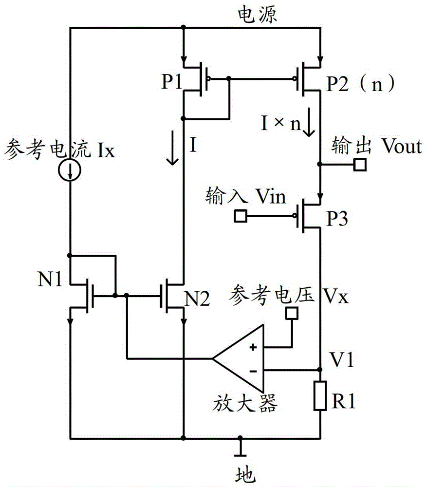
[0014] see figure 1 所示,为本发明的应用于音频放大器输入级的低失真电平位移缓冲电路结构的电路图。

[0015] 在一种实施方式中,该应用于音频放大器输入级的低失真电平位移缓冲电路结构包括参考电流源、第一N型MOS场效应管(N1)、第二N型MOS场效应管(N2)、第一P型MOS场效应管(P1)、第二P型MOS场效应管(P2)电路模块、第三P型MOS场效应管(P3)、电阻(R1)和运算放大器。

[0016] 其中,所述的第一N型MOS场效应管(N1)的栅极和漏极短接并连接到所述的参考电流源的一端,所述的参考电流源的另一端连接电源;所述的第一N型MOS场效应管(N1)的源极和衬底接地;所述的第二N型MOS场效应管(N2)的栅极连接所述的第一N型MOS场效应管(N1)的栅极;所述的第二N型MOS场效应管(N2)的漏极连接所述的第一P型MOS场效应管(P1)的相互短接的栅极和漏极;所述的第二N型MOS场效应管(N2)的源极和衬底接地;所述的第一P型MOS场效应管(P1)的源极和衬底连接所述的电源;所述的第二P型MOS场效应管(P2)的栅极连接所述的第一P型MOS场效应管(P1)的栅极;所述的第二P型MOS场效应管(P2)的源极和衬底连接所述的电源;所述的第二P型MOS场效应管(P2)的漏极连接所述的第三P型MOS场效应管(P3)的源极和衬底,并为该电路结构的输出节点(Vout);所述的第三P型MOS场效应管(P3)的栅极为该电路结构的输入节点(Vin);所述的第三P型MOS场效应管(P3)的漏极连接所述的运算放大器的反向输入端,并通过所述的电阻(R1)接地;所述的运算放大器的正向输入端连接外部参考电压(Vx);所述的运算放大器的输出端连接所述的第一N型MOS场效应管(N1)和第二N型MOS场效应管(N2)的栅极。

[0017] 在一种较优选的实施方式中,所述的第一N型MOS场效应管(N1)与所述的第二N型MOS场效应管(N2)的沟道宽长比相同。所述的第一P型MOS场效应管(P1)与所述的第二P型MOS场效应管(P2)电路模块的沟道宽长比也相同。

[0018] 在一种更优选的实施方式中,所述的第二P型MOS场效应管(P2)电路模块由20至5...


PUM


Abstract

The invention relates to a low-distortion level-shift buffer circuit structure applied to the input stage of an audio amplifier, and belongs to the technical field of circuit structures. In this circuit structure, the current I flowing through N1 and N2 is determined by the value of the reference voltage Vx and the resistor R1 and has nothing to do with the amplitude of the input signal, which eliminates the signal distortion caused by the channel length modulation effect of P2. When the output signal is in When it fluctuates within a reasonable range, the current flowing through P3 remains unchanged, ensuring good linearity of the output signal; at the same time, since P2 is composed of multiple P-type MOS field effect transistors in parallel, the transconductance gm2 of each P-type MOS field effect transistor is very small, and due to the introduction of feedback, the characteristics of P2 are close to the ideal current source, so the noise generated by P2 is greatly reduced, so that the low-distortion level-shift buffer circuit structure applied to the audio amplifier input stage of the present invention satisfies For the requirements of low noise and good linearity, and its simple structure, the cost is relatively low.

Description

technical field [0001] 本发明涉及电路结构技术领域,特别涉及放大器输入级电路结构领域,具体是指一种应用于音频放大器输入级的低失真电平位移缓冲电路结构。 Background technique [0002] 在CMOS集成电路工艺中源跟随器由于其本身具有极高的输入阻抗所以很适合用作电压缓冲级使得整个放大器获得更高的电压增益。但是源跟随器本身会引入显著的噪声,由于体效应或者沟道长度调制效应导致的非线性,由于电平移动导致输出电压摆幅的减小等等这些缺点限制了其在放大器中的使用。 [0003] 所以目前在放大器中源跟随器最普遍的应用是作为缓冲级完成电平位移的功能,特别是在放大器的输入级。因为在很多实际的应用场合音频放大器的输入端被要求偏置在地电平或者和地电平接近的较低的电压水平,这就要求在音频放大器的输入端和音频放大器之间加入一个源跟随器来先将输入信号的电平抬高。但是如前所述,由于源跟随器本身会引入显著的噪声和非线性所以限制了其在很多领域中的应用。 Contents of the invention [0004] 本发明的目的是克服了上述现有技术中的缺点,提供一种基于CMOS集成电路工艺,采用源跟随器实现音频信号的电平位移,同时满足放大器对于低噪声和良好线性度的要求,且结构简单,成本低廉的应用于音频放大器输入级的低失真电平位移缓冲电路结构。 [0005] 为了实现上述的目的,本发明的应用于音频放大器输入级的低失真电平位移缓冲电路结构具有如下构成: [0006] 该电路结构包括参考电流源、第一N型MOS场效应管(N1)、第二N型MOS场效应管(N2)、第一P型MOS场效应管(P1)、第二P型MOS场效应管(P2)电路模块、第三P型MOS场效应管(P3)、电阻(R1)和运算放大器;所述的第一N型MOS场效应管(N1)的栅极和漏极短接并连接到所述的参考电流源的一端,所述的参考电流源的另一端连接电源;所述的第一N型MOS场效应管(N1)的源极和衬底接地;所述的第二N型MOS场效应管(N2)的栅极连接所述的第一N型MOS场效应管(N1)的栅极;所述的第二N型MOS场效应管(N2)的漏极连接所述的第一P型MOS场效应管(P1)的相互短接的栅极和漏极;所述的第二N型MOS场效应管(N2)的源极和衬底接地;所述的第一P...

Claims


Application Information

Patent Timeline
Patent Type & Authority Patents(China)
IPC IPC(8): H03F1/26H03F1/32
Inventor 周景晖
Owner CRM ICBG (WUXI) CO LTD
Why Eureka
Try Eureka