

Chip structure of a plc multimode waveguide optical splitter
A chip structure, multi-mode optical waveguide technology, applied in the field of integrated optics, can solve the problem of no multi-mode shunt device, and achieve the effects of small size, good mechanical shock resistance, and convenient installation
- Summary
- Abstract
- Description
- Claims
- Application Information
AI Technical Summary
Problems solved by technology
Method used
Image

Examples
Embodiment 1
[0020] A chip structure of a PLC multimode waveguide optical splitter, including a glass substrate and a glass cover, the glass cover is set on the glass substrate and bonded by a UV adhesive layer, and the inside of the glass substrate is buried with Optical waveguide; the optical waveguide is a multi-mode optical waveguide, which multi-channel distributes the optical energy input by the multi-mode optical fiber, and the functional structure includes 1×N-type optical waveguide or 2×N-type optical waveguide, wherein N=2, 4, 8, 16 or 32. The diameter of the multimode optical waveguide is 30-350 μm,
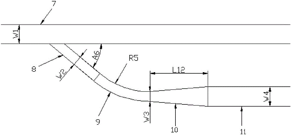
[0021] When N=2 in the 1×N type optical waveguide, its structure is as follows figure 1 As shown, it consists of main waveguide 7, side branch waveguide 8, arc waveguide 9, horn-shaped waveguide 10 and side output waveguide 11 connected in sequence, wherein side branch waveguide 8 is set on main waveguide 7, and the width of main waveguide 7 is W1 is 15 μm; the width W4 of the si...
Embodiment 2
[0028] see figure 1 , when N=2 in the 1×N type optical waveguide, it consists of the main waveguide 7, the side branch waveguide 8, the arc waveguide 9, the horn-shaped waveguide 10 and the side output waveguide 11 connected in sequence, wherein the side branch waveguide 8 is arranged on the main waveguide 7, the width W1 of the main waveguide 7 is 350 μm; the width W4 of the side output waveguide 11 is 350 μm.
[0029] The angle A6 between the main waveguide 7 and the side branch waveguide 8 is 0.5-15 degrees; the width W2 of the side branch waveguide 8 is 350 μm.
[0030] The value range of the width W3 of the arc waveguide 9 is 350 μm, and the range of its curvature radius R5 is 100000 μm.
[0031] The width of the thin end of the horn-shaped waveguide 10 is the same as W3, the width of the thick end is the same as W4, and the range of its length L12 is 40000 μm.
[0032] The ends of the main waveguide 7 and the side output waveguide 11 are each connected to one of the mu...
Embodiment 3
[0035] When N=2 in the 1×N-type optical waveguide, its structure can be found in figure 1 , consists of a main waveguide, and successively connected side branch waveguides, arc waveguides, horn-shaped waveguides and side output waveguides, wherein the side branch waveguides are set on the main waveguide, and the width W1 of the main waveguide is 150 μm; the width W4 of the side output waveguide is 150 μm.
[0036] The angle A6 between the main waveguide and the side branch waveguide is 10 degrees; the width W2 of the side branch waveguide is 100 μm.
[0037] The range of the width W3 of the arc waveguide is 150 μm, and the range of the radius of curvature R5 is 10000 μm.
[0038] The thin end width of the horn-shaped waveguide is the same as W3, the thick end width is the same as W4, and the range of its length L12 is 10000 μm. All the other are with embodiment 1.
PUM
 Abstract
Description
Claims
Application Information