
Semiconductor light-emitting diode chip

A technology of light-emitting diodes and semiconductors, applied in the direction of semiconductor devices, electrical solid devices, electrical components, etc., can solve the problems of low chip brightness, pad adhesion, etc., and achieve the goal of increasing area, increasing adhesion, and improving reliability Effect

Active Publication Date: 2014-03-05
YANGZHOU ZHONGKE SEMICON LIGHTING
View PDF4 Cites 8 Cited by
  • Summary
  • Abstract
  • Description
  • Claims
  • Application Information

AI Technical Summary

Problems solved by technology

[0005] In order to solve the problems of low brightness and pad adhesion caused by the loss of the light-emitting area of ​​the chip in the prior art, the present invention proposes a light-emitting diode chip structure

Method used


Image

  • Semiconductor light-emitting diode chip
  • Semiconductor light-emitting diode chip
  • Semiconductor light-emitting diode chip

Examples


Embodiment Construction

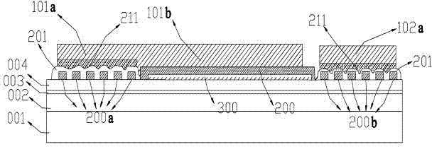
[0018] Such as figure 1 , 2 , 3 shown: on the narrow side L (such as image 3 As shown) on a rectangular substrate 001 less than 300um, an N-type semiconductor layer 002, a light-emitting composite layer 003 and a P-type semiconductor layer 004 are arranged in sequence, and the N-type semiconductor layer 002 is exposed in the middle of the P-type semiconductor layer 004 by etching. P pads 101 a and N pads 102 a are respectively provided on the P-type semiconductor layer 004 on both sides of the rectangular substrate 001 .

[0019] Patterned current spreading layers 200a and 200b are respectively disposed on the P-type semiconductor layer 004 corresponding to the P pad 101a and the N pad 102a, and the electrical insulating layer 201 is respectively disposed on the patterned current spreading layers 200a and 200b.

[0020] Reflectors 211 are respectively provided on the back of the P pad 101a and the back of the N pad 102a.

[0021] The P pads 101a are electrically connected ...


PUM


Abstract

The invention discloses a semiconductor light-emitting diode chip and relates to the technical field of light-emitting diode production. Corresponding graphical current expanding layers are arranged below an N welding disc and a P welding disc respectively, electronic recombination luminescence exists in all light-emitting recombination regions, the area of the light-emitting recombination regions is increased on the basis of the prior art, and chip current distribution and light-emitting luminance can be effectively improved; meanwhile, graphical current expansion can effectively increase surface adhesion force of the welding discs, and reliability of the chip can be improved.

Description

technical field [0001] The invention relates to the technical field of production of light-emitting diodes, in particular to the production technology of light-emitting diode chips. Background technique [0002] With the advancement of epitaxial technology, the brightness of semiconductor light-emitting diodes has increased year by year. Chips can be divided into high-power, medium-power, and low-power according to power; high-power faces large-size chips, but the large-size, high-power, and brightness 5 years ago can now be replaced by medium-sized chips, which cost less and go in turn. Medium-sized and medium-power chips can be replaced by existing small-sized chips; at the same time, the nitride semiconductor used to grow the epitaxial layer is not a perfect crystal. During the growth process, due to the different growth conditions of the layer and the layer, the crystal mismatch introduces defects. The defect density is about 10 9 cm -2 ~10 10 cm -2 , even if ...

Claims


Application Information

Patent Timeline
Patent Type & Authority Applications(China)
IPC IPC(8): H01L33/62H01L33/14H01L33/10
CPCH01L24/10H01L33/14H01L33/62H01L2224/10
Inventor 金豫浙冯亚萍张溢李佳佳李志聪孙一军王国宏
Owner YANGZHOU ZHONGKE SEMICON LIGHTING
Learn More