BICMOS circuit converting ECL logic level into MOS logic level

A MOS logic, logic level technology, applied in the direction of logic circuit connection/interface arrangement, logic circuit coupling/interface using field effect transistors, etc.

Inactive Publication Date: 2014-03-05
SUZHOU BATELAB MICROELECTRONICS
View PDF6 Cites 1 Cited by
  • Summary
  • Abstract
  • Description
  • Claims
  • Application Information

AI Technical Summary

Problems solved by technology

In the end, what is needed is a converter that can be used in a wide variety of situations whe

Method used


Image

  • BICMOS circuit converting ECL logic level into MOS logic level
  • BICMOS circuit converting ECL logic level into MOS logic level
  • BICMOS circuit converting ECL logic level into MOS logic level

Examples


Embodiment Construction

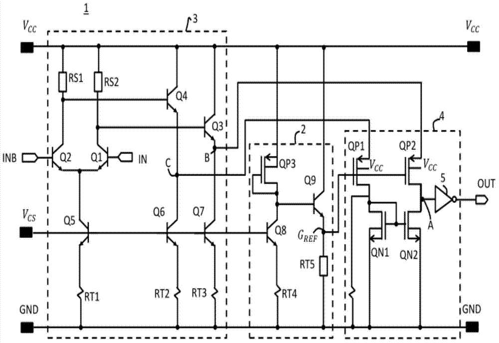
[0023] The device of the present invention, ECL to CMOS converter 1, in figure 2 is illustrated, including the reference voltage stage 2, used to develop an independent voltage reference source for the ECL to CMOS converter. It should be understood that the converter circuits described here can also be used in phase locked loop circuits, clock recovery circuits, or other circuit designs requiring fast converters. about figure 2 , an ECL input stage 3 of the ECL to CMOS converter 1, comprising a first input transistor Q1 and a second input transistor Q2, the first input transistor Q1 receives the first input signal IN on its control node, the second input transistor Q2 receives at its control node a second input signal INB which complements the first input signal IN. Preferably, Q1 and Q2 are connected to the high potential supply rail V CC .

[0024] The bipolar ECL input stage 3 further includes a first emitter follower transistor Q3 and a second emitter follower Q4, th...


PUM


Abstract

The invention discloses a BICMOS circuit converting an ECL logic level into an MOS logic level. The conversion circuit is used for converting the range of a first logic level into the range of a second logic level, just like the commonly-revolved phenomenon that the ECL stage is converted into the CMOS stage.

Description

Technical field: [0001] The present invention relates to a switching circuit for switching between different logic levels. In particular, the present invention relates to a switching circuit associated with emitter coupled logic (ECL) circuits for switching between logic levels associated with complementary metal oxide semiconductor (CMOS) circuits. More specifically, the present invention relates to a conversion circuit that generates a reference voltage that provides minimal delay for ECL to CMOS logic level conversion. Background technique: [0002] In the field of rapidly expanding circuits, it is necessary to take advantage of the desirable properties of bipolar and MOS transistors to provide smooth and fast transitions between different logic level voltage ranges associated with two transistors. In particular, bipolar transistors, which are known for their fast switching speeds between logic high and logic low, also dissipate power to a range where they cannot be used...

Claims


Application Information

Patent Timeline
IPC IPC(8): H03K19/0185
Inventor 不公告发明人
Owner SUZHOU BATELAB MICROELECTRONICS
Why Eureka
Try Eureka