One-dimensional nanomaterial welding method based on electrically-induced heating effect

A technology of nanomaterials and welding methods, applied in the field of nanomaterials

Inactive Publication Date: 2014-03-12
HEFEI INSTITUTES OF PHYSICAL SCIENCE - CHINESE ACAD OF SCI
View PDF6 Cites 5 Cited by
  • Summary
  • Abstract
  • Description
  • Claims
  • Application Information

AI Technical Summary

Problems solved by technology

But they also have many problems and deficiencies: the first is to affect the intrinsic performance of the device: for example, when the electrode is constructed by FIB, there is an ion source that pollutes the sample, leaving ion sources such as Ga atoms and other elements in the processed nanostructure; Second, because EBL needs to introduce exposure technology, its process is complicated, and it also pollutes the sample to a certain extent.

Method used


Image

  • One-dimensional nanomaterial welding method based on electrically-induced heating effect
  • One-dimensional nanomaterial welding method based on electrically-induced heating effect
  • One-dimensional nanomaterial welding method based on electrically-induced heating effect

Examples


Embodiment 1

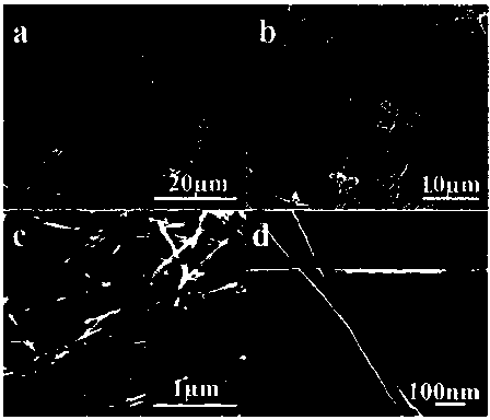
[0040] 1. Dispersion: Disperse 100μg of Cu nanowires with a diameter of 10nm and an average length of about 20μm in 100ml ethanol solution, and oscillate ultrasonically in an ultrasonic oscillator with a power of 10mW for 5 minutes; surface of the silicon wafer. Then place the silicon wafer at room temperature, and after the solvent evaporates, the one-dimensional nanomaterials can be dispersed on the silicon wafer; figure 1 As shown, the Cu nanowires dispersed on the silicon wafer were magnified by 5000 times, 8000 times and 100000 times, respectively, as shown in the SEM images figure 1 Shown in a-c; its perspective electron microscope picture is shown in figure 1 Shown in d. It shows that the Cu nanowires are dispersed on the silicon wafer, which is convenient for the pick-up of the subsequent single-track nanowires;

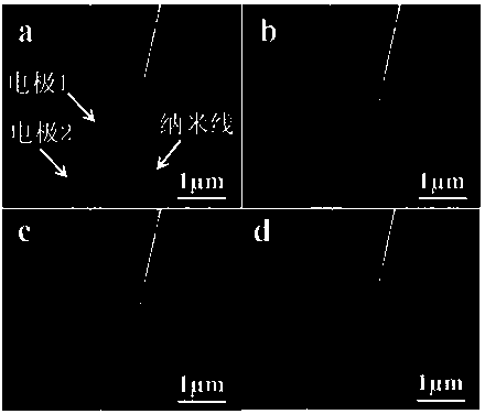
[0041] 2. Selection: Under the scanning electron microscope, select a Cu nanowire, use the nano-manipulation probe to pick it up and transfer it to ano...

Embodiment 2

[0048] 1. Dispersion: Disperse 100 μg of Cu nanotubes with a diameter of 15 nm and an average length of about 5 μm in 50 ml of water, and oscillate ultrasonically for 15 minutes in an ultrasonic oscillator with a power of 10 mW. After the dispersion is uniform, take 10 μL of the dispersion and drop it on the surface of a clean silicon wafer. Then place the silicon wafer at room temperature, and after the solvent evaporates, the one-dimensional nanomaterials can be dispersed on the silicon wafer;

[0049] 2. Selection: Under the scanning electron microscope, select a Cu nanotube, use the nano-manipulation probe to pick it up and transfer it to another silicon wafer substrate with Ag electrodes, and place it on the place to be welded;

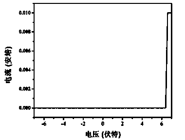
[0050] 3. Welding: Use two tungsten probe electrodes with a radius of curvature of 500nm, one of which is pressed on the surface of the Cu nanotube, and the other is pressed on the Ag conductive layer of the silicon wafer near the Cu nanowire, an...

Embodiment 3

[0053] 1. Dispersion: Disperse 200 μg of Ag nanowires with a diameter of 80 nm and an average length of about 15 μm in 10 ml of methanol, and oscillate ultrasonically for 30 minutes in an ultrasonic oscillator with a power of 30 mW. After the dispersion is uniform, take 10 μL of the dispersion and drop it on the surface of a clean silicon wafer. Then place the silicon wafer at room temperature, and after the solvent evaporates, the one-dimensional nanomaterials can be dispersed on the silicon wafer;

[0054] 2. Selection: Under the scanning electron microscope, select an Ag nanowire, use the nano-manipulation probe to pick it up and transfer it to another glass substrate with Ag electrodes, and place it on the place to be welded;

[0055] 3. Welding: Use two tungsten probe electrodes with a radius of curvature of 500nm, one of which is pressed on the surface of the Ag nanowire, and the other is pressed on the Ag conductive layer of the glass substrate near the nanowire, and ap...


PUM

PropertyMeasurementUnit
diameteraaaaaaaaaa
radiusaaaaaaaaaa
radiusaaaaaaaaaa

Abstract

The invention discloses a one-dimensional nanomaterial welding method based on the electrically-induced heating effect. According to the method, a voltage of certain waveform and size is exerted through a probe electrode, and a one-dimensional nanomaterial is welded onto a base provided with an electrode. According to the method, by means of electrically-induced heating of the one-dimensional nanomaterial, the joint part of a conducting film on the base and the one-dimensional nanomaterial is partially and mutually melted so as to achieve the welding effect, and the bonding strength between the one-dimensional nanomaterial and the base is higher than 50nN. According to the method, the welding position of the one-dimensional nanomaterial can be selected and controlled accurately, welding spots are small, the accuracy is high, no other welding materials need to be introduced, samples cannot be polluted, and the method plays a key role in promoting development of nanoelectronics.

Description

technical field [0001] The invention relates to the technical field of nanometer materials, in particular to a welding method between a one-dimensional nanometer material and a substrate with electrodes based on the electrothermal effect. Background technique [0002] In recent years, with the continuous advancement of nanotechnology, people have been able to easily prepare tens of thousands of nanomaterials through various physical, chemical or biological methods, among which one-dimensional nanomaterials are characterized by their unique electrical properties and their novel The application potential in very large scale integrated circuits has received a lot of attention from all walks of life. Based on a single one-dimensional nanomaterial, welding it with nano-device units to form nano-electronic devices with special functions and functions, building circuits and new sensors has become a worldwide frontier topic. Difficulties in welding due to the incompatibility betwee...

Claims


Application Information

Patent Timeline
Patent Type & Authority Applications(China)
IPC IPC(8): B23K11/16B82B3/00
CPCB23K11/16B23K11/34B23K35/0205B23K35/222B82B3/00
Inventor 金震
Owner HEFEI INSTITUTES OF PHYSICAL SCIENCE - CHINESE ACAD OF SCI
Why Eureka
Try Eureka