Self-aligned double patterning formation method
A dual-patterning, self-aligning technology, applied in electrical components, semiconductor/solid-state device manufacturing, circuits, etc., can solve the problems of poor sidewall morphology of etched patterns and cumbersome processes, saving the etching process, sidewalls, etc. Better appearance
- Summary
- Abstract
- Description
- Claims
- Application Information
AI Technical Summary
Problems solved by technology
Method used
Image
Examples
Embodiment Construction
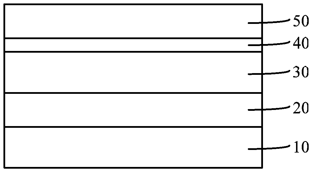
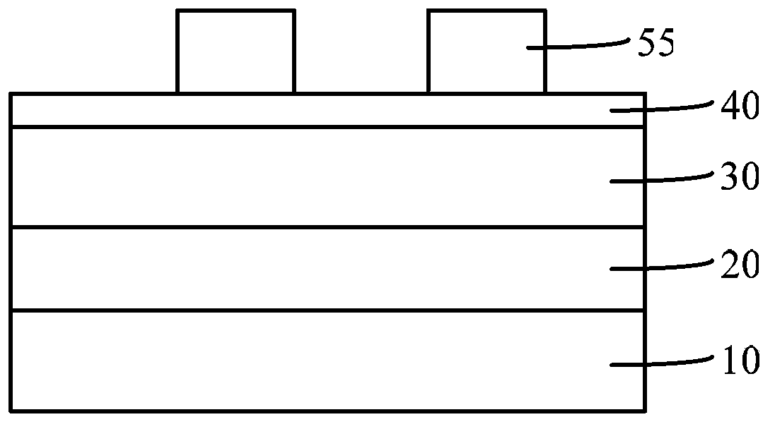
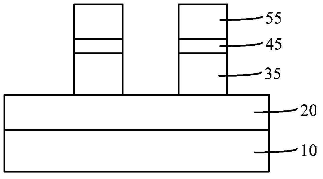
[0032] The sidewall morphology of the etched pattern formed by etching the material layer to be etched by the above-mentioned technique is relatively poor, and the process is cumbersome. After research, it is found that when the photoresist layer is exposed and developed to form a patterned photoresist layer, it is necessary to use the patterned photoresist layer as a mask to cover the bottom anti-reflection layer, sacrificial layer, etc. The material layer is dry etched. The dry etching step will cause damage to the topography of the patterned photoresist layer edge and the sidewall topography of the formed sacrificial layer, so that the sidewall shape of the mask sidewall formed on the sidewall surface of the sacrificial layer The appearance is not good, which affects the shape of the sidewall of the final etched material layer to be etched. Moreover, after exposing and developing the photoresist layer, it is necessary to etch and remove the bottom anti-reflective layer. Si...
PUM
 Abstract
Description
Claims
Application Information


