Formation method of semiconductor structure

A technology of semiconductor and gate structure, applied in the field of semiconductor structure formation, can solve the problems of deviation of design value, influence of conductive plug connection performance, influence of semiconductor structure performance, etc., to prevent the distance from being too close, good sidewall position accuracy accuracy and topographical accuracy, avoiding electrical connection problems

Active Publication Date: 2019-09-27
SEMICON MFG INT (SHANGHAI) CORP +1
View PDF4 Cites 0 Cited by
  • Summary
  • Abstract
  • Description
  • Claims
  • Application Information

AI Technical Summary

Problems solved by technology

[0004] In the prior art, during the formation of the semiconductor structure, the size of the contact hole formed by the self-alignment process is likely to deviate from the design value, which will affect the connection performance of the formed conductive plug and affect the performance of the formed semiconductor structure

Method used


Image

  • Formation method of semiconductor structure
  • Formation method of semiconductor structure
  • Formation method of semiconductor structure

Examples


Embodiment Construction

[0032] It can be seen from the background art that the performance of the semiconductor structure formed in the prior art needs to be improved.

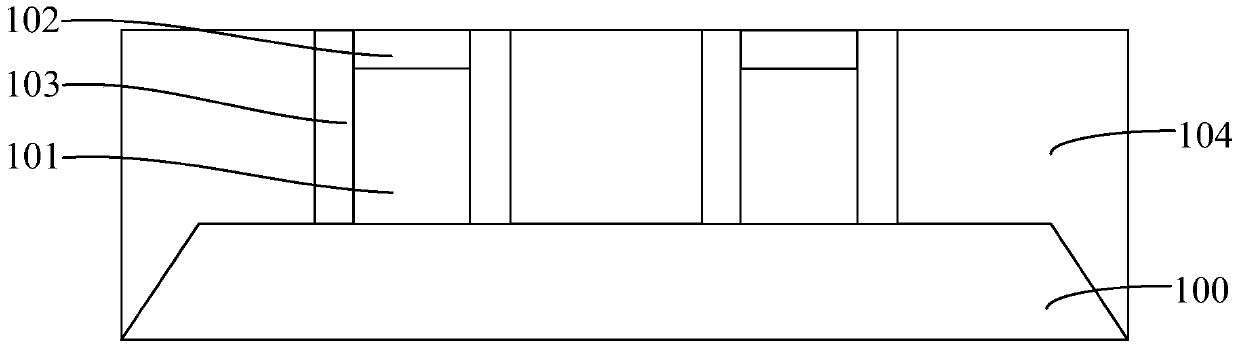
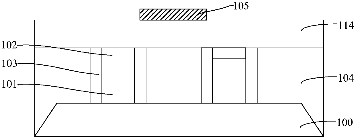
[0033] Figure 1 to Figure 7 It is a structural schematic diagram of a process of forming a semiconductor structure provided by an embodiment.

[0034] refer to figure 1 , provide a substrate 100, the surface of the substrate 100 forms a number of discrete gate structures, the gate structure includes: a gate 101, a hard mask layer 102 located on the surface of the gate 101, the gate structure also includes a cover gate The sidewall surface of the pole 101 and the sidewall 103 on the sidewall surface of the hard mask layer 102 . The surface of the substrate 100 is further formed with a first dielectric layer 104 covering the sidewall surface of the gate structure, and the top of the first dielectric layer 104 is flush with the top of the gate structure.

[0035] Wherein, the gate 101 includes a gate dielectric layer and a gate elec...


PUM


Abstract

The invention provides a formation method of a semiconductor structure. The formation method comprises the steps that a first mask layer crossing a dielectric layer between the adjacent gate structures is formed on the surface of the dielectric layer; a side wall layer is formed on the surface of the sidewall of the first mask layer on the surface of the dielectric layer between the adjacent gate structures; a second mask layer having an opening is formed on the surface of the first mask layer and the surface of the dielectric layer, and the opening crosses the first mask layer and the side wall layer; the dielectric layer exposed out of the side wall layer and the first mask layer is etched along the opening with the second mask layer acting as the mask until the surface of a substrate is exposed, and discrete contact holes are formed in the dielectric layer between the adjacent gate structures; the second mask layer and the first mask layer are removed; and conductive plugs fully filling in the contact holes are formed. The sidewall position accuracy and the shape accuracy of the formed contact holes are improved so as to enhance the electrical performance and the yield rate of the formed semiconductor structure.

Description

technical field [0001] The invention relates to the technical field of semiconductor manufacturing, in particular to a method for forming a semiconductor structure. Background technique [0002] With the continuous development of semiconductor process technology, such as the introduction of high-K gate dielectric layer, stress engineering technology, pocket ion implantation, and continuous optimization of materials and device structures, the size of semiconductor devices continues to shrink. However, when the feature size of the device is further reduced, planar transistors face huge challenges due to the more significant short-channel effect, process variation, and reduced reliability. Compared with planar transistors, FinFETs have fully depleted fins, lower dopant ion concentration fluctuations, higher carrier mobility enhancement, lower parasitic junction capacitance, and higher area usage efficiency has received extensive attention. [0003] In the integrated circuit m...

Claims


Application Information

Patent Timeline
Patent Type & Authority Patents(China)
IPC IPC(8): H01L21/768H01L21/336
Inventor 张城龙洪中山
Owner SEMICON MFG INT (SHANGHAI) CORP
Why Eureka
Try Eureka