High power square thyristor packaging structure

A high-power, square-chip technology, applied in electrical components, electrical solid-state devices, circuits, etc., can solve the problems of delamination between the silicone protective layer and the chip, low working reliability, and poor moisture resistance, and achieve product moisture resistance. Enhancement, increased work reliability, avoids the effect of stratification

Active Publication Date: 2016-02-24
江苏东晨电子科技有限公司
View PDF5 Cites 0 Cited by
  • Summary
  • Abstract
  • Description
  • Claims
  • Application Information

AI Technical Summary

Problems solved by technology

[0003] At present, the packaging structure of high-power square thyristors is usually packaged in a silicone or resin protective material connected up and down, and the chip is soldered to the position to be installed by solder. The silicone or resin protective material around the chip is directly connected to the chip. In contact with solder, it is easy to cause delamination between the silicone protective layer and the chip, the product has poor moisture resistance, low reliability, and is easy to damage

Method used


Image

  • High power square thyristor packaging structure

Examples


Embodiment Construction

[0014] The present invention will be further described below in conjunction with the accompanying drawings and embodiments.

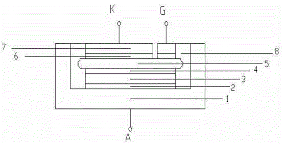
[0015] Such as figure 1 As shown, a high-power square thyristor packaging structure, which includes an upper molybdenum sheet 7, a third solder layer 6, a chip 5, a second solder layer 4, a lower molybdenum sheet 3 and a first molybdenum sheet arranged sequentially from top to bottom A solder layer 2, the aforementioned upper molybdenum sheet 7, the third solder layer 6, the chip 5, the second solder layer 4, the lower molybdenum sheet 3 and the first solder layer 2 are all placed in the silica gel frame 8, and the two ends of the chip 5 are inserted into the Inside the silicone frame 8, a conductive shell 1 is installed outside the silicone frame 8. The conductive shell 1 is a semi-enclosed structure with the top open and the other three sides closed. The bottom of the conductive shell 1 is welded on the high-power square piece. Where the silicon need...


PUM


Abstract

A high-power square-piece silicon controlled rectifier packaging structure comprises an upper molybdenum plate (7), a third welding flux layer (6), a chip (5), a second welding flux layer (4), a lower molybdenum plate (3) and a first welding flux layer (2) which are sequentially arranged from top to bottom, wherein the upper molybdenum plate (7), the third welding flux layer (6), the chip (5), the second welding flux layer (4), the lower molybdenum plate (3) and the first welding flux layer (2) are arranged in a silica gel frame (8), two ends of the chip (5) are inserted into the silica gel frame (8), a conductive casing (1) is installed outside the silica gel frame (8), the top of the conductive casing (1) is open, the other three sides are of semi-surrounded structures, and the bottom of the conductive casing (1) is welded at the position where a high-power square-piece silicon controlled rectifier is required to be installed. When the high-power square-piece silicon controlled rectifier packaging structure is used, the assembling operation is simple and easy. Compared with traditional packaging modes, the reject ratio is reduced by one magnitude order.

Description

technical field [0001] The invention relates to a thyristor packaging structure, in particular to a high-power square chip thyristor packaging structure. Background technique [0002] Thyristor, the abbreviation of silicon controlled rectifier element, is a high-power semiconductor device with a four-layer structure of three PN junctions, also known as a thyristor. With the characteristics of small size, relatively simple structure, and strong functions, it is one of the more commonly used semiconductor devices. The device is widely used in various electronic equipment and electronic products, and is mostly used for controllable rectification, inverter, frequency conversion, voltage regulation, non-contact switch, etc. [0003] At present, the packaging structure of high-power square thyristors is usually packaged in a silicone or resin protective material connected up and down, and the chip is soldered to the position to be installed by solder. The silicone or resin protec...

Claims


Application Information

Patent Timeline
Patent Type & Authority Patents(China)
IPC IPC(8): H01L23/31
Inventor 许志峰
Owner 江苏东晨电子科技有限公司
Why Eureka
Try Eureka