
System for achieving capacitance detection and electromagnetic detection

A technology of capacitance detection and electromagnetic detection, applied in the direction of electrical digital data processing, input/output process of data processing, instruments, etc., can solve the problems of complex structure, large volume and high production cost of touch products, and ensure the transmission and reception And the detection of electromagnetic signals, avoiding mutual interference, and the effect of simplifying the structure

Inactive Publication Date: 2014-03-26
TELINK SEMICON SHANGHAI
View PDF4 Cites 18 Cited by
  • Summary
  • Abstract
  • Description
  • Claims
  • Application Information

AI Technical Summary

Problems solved by technology

[0006] At present, in order to realize the dual touch of hand and pen, the capacitive touch mode and the electromagnetic touch mode are superimposed and used together to realize the touch mode combining handwriting and pen writing. The touch area of ​​the capacitive touch mode It needs to be set on the touch area of ​​the electromagnetic touch mode, that is to say, two mutually independent array structures need to be set on the same touch device and superimposed on each other, so that the position of the two modes can be realized. However, each array circuit needs to be connected to its own processing circuit, which makes the whole touch product complex in structure, large in size, high in production cost, and in the process of using the touch product, there will be capacitive touch control mode and electromagnetic touch mode; in addition, the capacitive touch drive electrodes and capacitive touch sensing electrodes are fabricated on one chip, and the electromagnetic antenna board is fabricated on another chip, resulting in a thicker finished product, which does not meet current requirements. Market demand, and the cost is high

Method used


Image

  • System for achieving capacitance detection and electromagnetic detection
  • System for achieving capacitance detection and electromagnetic detection
  • System for achieving capacitance detection and electromagnetic detection

Examples


Embodiment Construction

[0040] In order to make the object, technical solution and advantages of the present invention clearer, various embodiments of the present invention will be described in detail below in conjunction with the accompanying drawings. However, those of ordinary skill in the art can understand that, in each implementation manner of the present invention, many technical details are provided for readers to better understand the present application. However, even without these technical details and various changes and modifications based on the following implementation modes, the technical solution claimed in each claim of the present application can be realized.

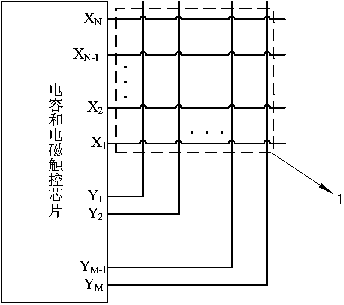
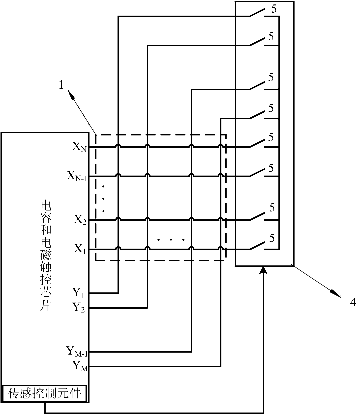
[0041] The first embodiment of the present invention relates to a system for realizing capacitive detection and electromagnetic detection. It includes touch screen panel, capacitive and electromagnetic touch chip, sensor antenna multiplexing array (wire array with both sensor and antenna functions), switch array.

[0042] S...


PUM


Abstract

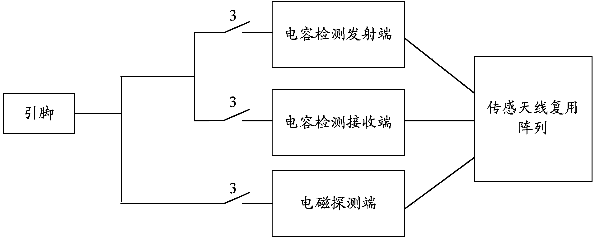
The invention relates to the field of touch control and discloses a system for achieving capacitance detection and electromagnetic detection. A transverse row of wires and a vertical row of wires included by a sensing antenna multiplex array are located in a touch area of a touch control screen panel, a capacitance and electromagnetic touch control chip is provided with a TX end, an RX end and an EM Detect end, one end of the TX end, one end of the RX end and one end of the EM Detect end are respectively provided with one chip lead in a multiplex mode, and the other end of the TX end, the other end of the RX end and the other end of the EM Detect end are connected with one end of the transverse row of the wires and one end of the vertical row of the wires. When capacitance touch detection is carried out on the system, all switches in a switch array are turned off, and the transverse row of the wires and the vertical row of the wires constitute sensors of a capacitance screen; when electromagnetic touch detection is carried out on the system, all the switches are turned on, and the transverse row of the wires and the vertical row of the wires constitute antenna loops of an electromagnetic screen; when a part of the switches are turned off and a part of the switches are turned on, a part of the transverse row of the wires and a part of the vertical row of the wires constitute the sensors of the capacitance screen, and a part of the transverse row of the wires and a part of the vertical row of the wires constitute the antenna loops of the electromagnetic screen. Compared with the prior art, time division multiplex access of capacitance detection and electromagnetic detection is achieved through one set of sensing antennas on the single chip.

Description

technical field [0001] The invention relates to the field of touch technology, in particular to a system for realizing capacitance detection and electromagnetic detection. Background technique [0002] As a special computer peripheral, the touch screen can provide a human-computer interaction interface between the electronic system and the user, and has been widely used in many fields, for example, in mobile phones, personal digital assistants (Personal Digital Assistant, PDA), Game consoles, liquid crystal displays (Liquid Crystal Display, LCD), plasma displays (Plasma Display Panel, PDP), etc. [0003] At present, touch screens mainly fall into the following categories: electromagnetic touch screens, capacitive touch screens, electrical touch screens, and infrared touch screens. [0004] Among them, the capacitive touch screen generally adopts a front-attached type, and a capacitive touch driving electrode and a capacitive touch sensing electrode of a transparent conducti...

Claims


Application Information

Patent Timeline
Patent Type & Authority Applications(China)
IPC IPC(8): G06F3/044G06F3/046
Inventor 谢循张耀国金海鹏郑明剑盛文军
Owner TELINK SEMICON SHANGHAI
Learn More