AMOLED pixel drive circuit, drive method and array drive system

A pixel drive circuit and drive method technology, applied in the field of array drive systems and AMOLED pixel drive circuits, can solve the problems of low luminous efficiency, small relative aperture, etc., achieve high luminous efficiency, increase relative aperture, and simple driving method

Active Publication Date: 2014-03-26
SHANGHAI ADVANCED RES INST CHINESE ACADEMY OF SCI
View PDF4 Cites 2 Cited by
  • Summary
  • Abstract
  • Description
  • Claims
  • Application Information

AI Technical Summary

Problems solved by technology

[0009] In view of the above-mentioned shortcomings of the prior art, the purpose of the present invention is to provide an AMOLED pixel drive circuit, a drive circuit and a drive method, which are used to solve the problem of small relative aperture due to the existence of capacitance in the AMOLED drive circuit in the prior art. Problems such as low luminous efficiency

Method used


Image

  • AMOLED pixel drive circuit, drive method and array drive system
  • AMOLED pixel drive circuit, drive method and array drive system
  • AMOLED pixel drive circuit, drive method and array drive system

Examples


Embodiment 1

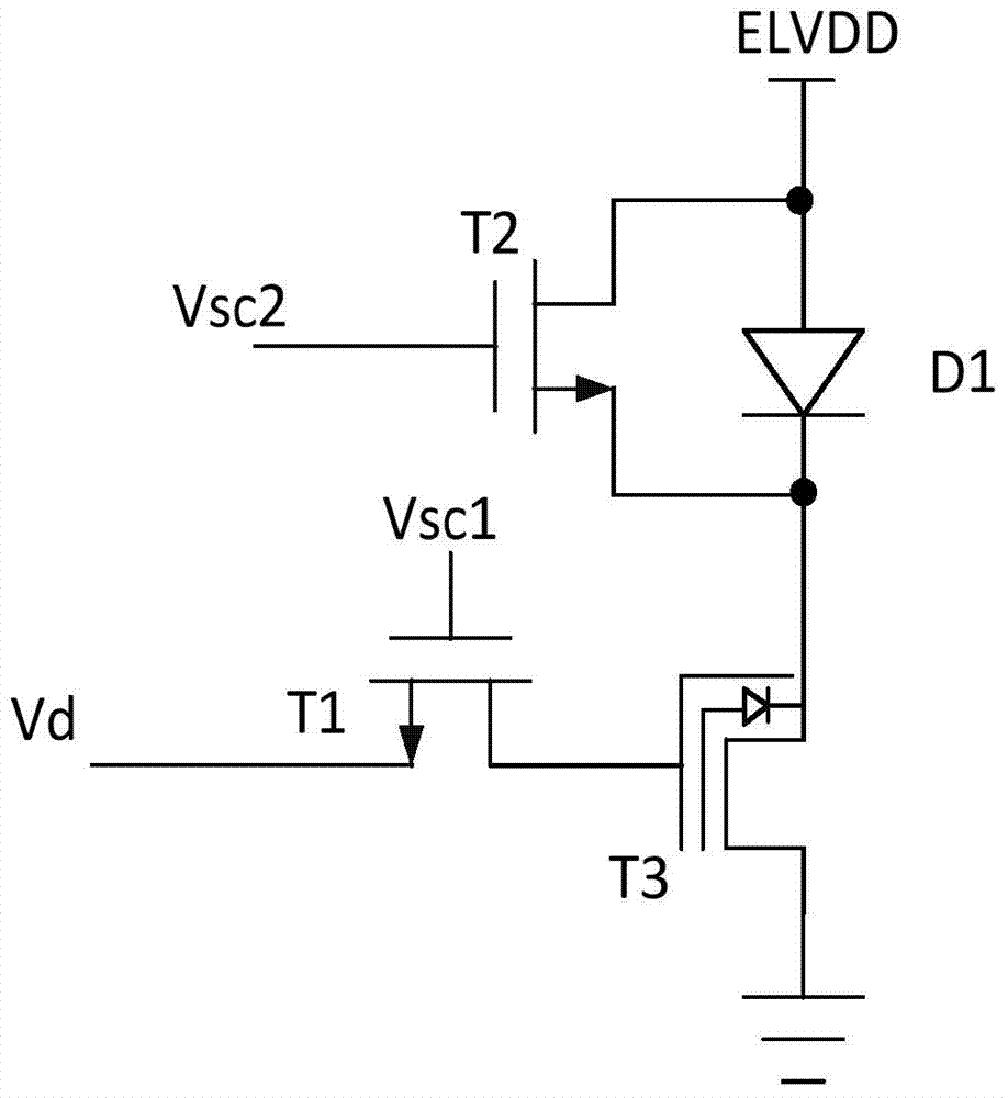
[0060] Such as Figure 2 ~ Figure 4 As shown, this embodiment provides an AMOLED pixel driving circuit, and the pixel driving circuit includes:

[0061] The first transistor T1, the second transistor T2, the organic light emitting diode D1 and the driving transistor T3, the driving transistor T3 includes a control gate and a semi-floating gate, and its threshold voltage is adjustable;

[0062] The gate of the first transistor T1 is connected to the first scanning signal Vsc1, the first electrode is connected to the data signal Vd, and the second electrode is connected to the control gate of the driving transistor T3; the source doped region of the driving transistor T3 is grounded, The doped drain region is connected to the first pole of the organic light emitting diode D1; the second pole of the organic light emitting diode D1 is connected to the external power supply ELVDD; the gate of the second transistor T2 is connected to the second scanning signal Vsc2, and the first T...

Embodiment 2

[0091] Such as Figure 5 As shown, this embodiment provides a driving circuit for an AMOLED pixel driving circuit, including:

[0092] A data signal driving circuit, used to generate a data signal Vd;

[0093] A scanning circuit, configured to generate a first scanning signal Vsc1 and a second scanning signal Vsc2;

[0094] The pixel array is formed by a plurality of AMOLED pixel drive circuits arranged in a matrix. The specific structure of the AMOLED pixel drive circuit is as described in Embodiment 1, wherein the plurality of pixel drive circuits share the same external power supply and ground wire, and each row The pixel driving circuits in each column share the first scanning signal Vsc1 and the second scanning signal Vsc2, and the pixel driving circuits in each column share the data signal Vd.

[0095] Such as Image 6 As shown, this embodiment also provides a driving method for the driving circuit of the AMOLED pixel driving circuit. Still taking the first transistor...


PUM


Abstract

The invention provides an AMOLED pixel drive circuit, a drive method and an array drive system. The AMOLED pixel drive circuit comprises a first transistor, a second transistor, an organic light emitting diode and a drive transistor, wherein a threshold voltage of the drive transistor can be adjusted. The grid of the first transistor is connected with a first scanning signal, the first electrode of the first transistor is connected with a data signal, and the second electrode of the first transistor is connected with a control grid of the drive transistor. A source doped region of the drive transistor is connected to the ground, and a drain doped region of the drive resistor is connected with the first pole of the organic light emitting diode. The second pole of the organic light emitting diode is connected with an external power source. The grid of the second transistor is connected with a second scanning signal, and the first electrode and the second electrode of the second transistor are connected with the first pole and the second pole of the organic light emitting diode respectively. According to the AMOLED pixel drive circuit, a traditional capacitor and a PMOS transistor are replaced by the drive transistor with the adjustable threshold voltage. Therefore, the relative aperture of the pixel drive circuit is greatly improved, and light-emitting efficiency of the pixel drive circuit is greatly improved.

Description

technical field [0001] The invention relates to a pixel driving technology of an OLED display, in particular to an AMOLED pixel driving circuit, a driving method and an array driving system. Background technique [0002] Active Matrix Organic Light Emitting Diode (AMOLED), compared with traditional passively driven Organic Light Emitting Diode (PMOLED), has the advantages of fast response time, high contrast, and large viewing angle, and has become the next generation display technology field in recent years. strong competitor. [0003] The most basic light-emitting pixel structure of AMOLED is 2T1C structure, which is composed of switching transistor T1, driving transistor T2, capacitor C1 and organic light-emitting diode D1, such as figure 1 shown. The gate of the switching transistor T1 is connected to the scanning signal Vscan, the drain is connected to the data signal Vdata, and the source is connected to the gate of the driving transistor T2 and the first pole of the...

Claims


Application Information

Patent Timeline
Patent Type & Authority Applications(China)
IPC IPC(8): G09G3/32G09G3/3233
Inventor 汪辉丁毅岭方娜汪宁章琦田犁封松林
Owner SHANGHAI ADVANCED RES INST CHINESE ACADEMY OF SCI
Why Eureka
Try Eureka