Method for improving surface damage of SOI (Silicon-On-Insulator) substrate
A substrate surface and substrate technology, applied in electrical components, semiconductor/solid-state device manufacturing, circuits, etc., can solve problems such as abnormal gate oxide growth, large fluctuations in circuit well resistance, and reduce substrate surface damage
- Summary
- Abstract
- Description
- Claims
- Application Information
AI Technical Summary
Problems solved by technology
Method used
Image

Examples
Embodiment 1
[0015] Embodiment 1: a method for improving SOI substrate surface damage, comprising the following process steps:
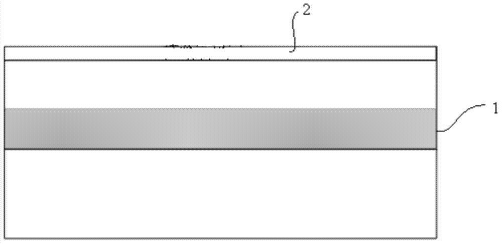
[0016] (1) Sacrificial oxidation: such as figure 1 As shown, the surface of the SOI substrate 1 is thermally oxidized to form a masking oxide layer 2 at a temperature of 850° C. for 30 minutes, and the thickness of the masking oxide layer is 15 nm;
[0017] (2) Reinforcement implantation: implant element Ar into the masking oxide layer, the implantation energy is 200 keV, and the implantation dose is 1×10 15 ;
[0018] (3) Cleaning: The SOI substrate was cleaned with conventional 3# and 1# cleaning solutions respectively. The cleaning temperature of 3# cleaning solution was 100 °C for 10 minutes, and the cleaning temperature of 1# cleaning solution was 70 °C. The cleaning time is 10 minutes; 3# cleaning liquid is made of H 2 SO 4 and H 2 o 2 It is obtained by mixing at a mass ratio of 3:1, and the 1# cleaning solution is made of NH 3 h 2 O, H 2 o 2 and ...
Embodiment 2
[0022] Embodiment two: a kind of method for improving SOI substrate surface damage, comprises following process step:
[0023] (1) Sacrificial oxidation: such as figure 1 As shown, the masking oxide layer 2 is formed by thermal oxidation on the upper surface of the SOI substrate 1 at a temperature of 840° C. for 31 minutes, and the thickness of the masking oxide layer is 14 nm;
[0024] (2) Reinforcement implantation: implant element Ar into the masking oxide layer, the implantation energy is 198 keV, and the implantation dose is 0.95×10 15 ;
[0025] (3) Cleaning: The SOI substrate was cleaned with conventional 3# and 1# cleaning solutions respectively. The cleaning temperature of 3# cleaning solution was 98 ° C for 11 minutes, and the cleaning temperature of 1 # cleaning solution was 68 ° C. The cleaning time is 11 minutes; 3# cleaning solution is made of H 2 SO 4 and H 2 o 2 It is obtained by mixing at a mass ratio of 3:1, and the 1# cleaning solution is made of NH 3...
Embodiment 3
[0029] Embodiment three: a method for improving SOI substrate surface damage, comprising the following process steps:
[0030] (1) Sacrificial oxidation: such as figure 1 As shown, the masking oxide layer 2 is formed by thermal oxidation on the upper surface of the SOI substrate 1 at a temperature of 860° C. for 29 minutes, and the thickness of the masking oxide layer is 16 nm;
[0031] (2) Reinforcement implantation: implant element Ar into the masking oxide layer, the implantation energy is 202 keV, and the implantation dose is 1.05×10 15 ;
[0032] (3) Cleaning: The SOI substrate was cleaned with conventional 3# and 1# cleaning solutions respectively. The cleaning temperature of 3# cleaning solution was 102 °C for 9 minutes, and the cleaning temperature of 1# cleaning solution was 72 °C. The cleaning time is 9 minutes; 3# cleaning liquid is made of H 2 SO 4 and H 2 o 2 It is obtained by mixing at a mass ratio of 3:1, and the 1# cleaning solution is made of NH 3 h 2 ...
PUM
| Property | Measurement | Unit |
|---|---|---|
| thickness | aaaaa | aaaaa |
| thickness | aaaaa | aaaaa |
| thickness | aaaaa | aaaaa |
Abstract
Description
Claims
Application Information
 - R&D
- Intellectual Property
- Life Sciences
- Materials
- Tech Scout
- Unparalleled Data Quality
- Higher Quality Content
- 60% Fewer Hallucinations
Browse by: Latest US Patents, China's latest patents, Technical Efficacy Thesaurus, Application Domain, Technology Topic, Popular Technical Reports.
© 2025 PatSnap. All rights reserved.Legal|Privacy policy|Modern Slavery Act Transparency Statement|Sitemap|About US| Contact US: help@patsnap.com