Method for preparing dual damascene structure

A dielectric layer and semiconductor technology, applied in semiconductor/solid-state device manufacturing, electrical components, circuits, etc., can solve problems such as no good trench filling method

Active Publication Date: 2014-03-26
SEMICON MFG INT (SHANGHAI) CORP
View PDF4 Cites 3 Cited by
  • Summary
  • Abstract
  • Description
  • Claims
  • Application Information

AI Technical Summary

Problems solved by technology

In order to solve this problem, in the prior art, there are also trenches in which sloped sidewalls are formed in the trenches to solve the problem, but vertical trench sidewalls or better VBD, TDDB performance, which contradicts the choice of sloped sidewalls for better fill
[0004] At present, there is no good trench filling method, which can make voids and gaps no longer appear in the filling process, and at the same time make the VBD and TDDB performance of semiconductor devices better

Method used


Image

  • Method for preparing dual damascene structure
  • Method for preparing dual damascene structure
  • Method for preparing dual damascene structure

Examples


Embodiment Construction

[0031] In the following description, numerous specific details are given in order to provide a more thorough understanding of the present invention. It will be apparent, however, to one skilled in the art that the present invention may be practiced without one or more of these details. In other examples, some technical features known in the art are not described in order to avoid confusion with the present invention.

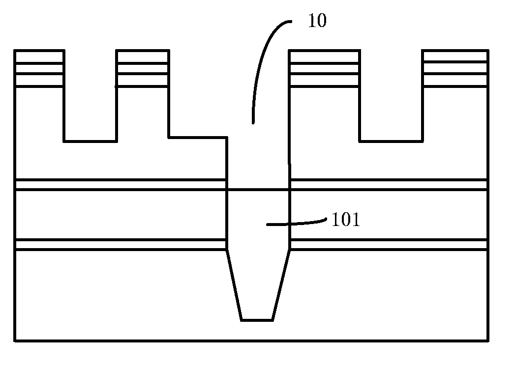
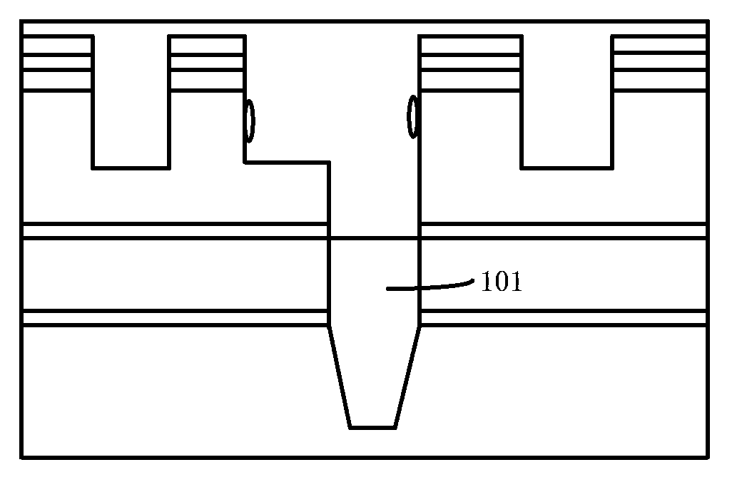
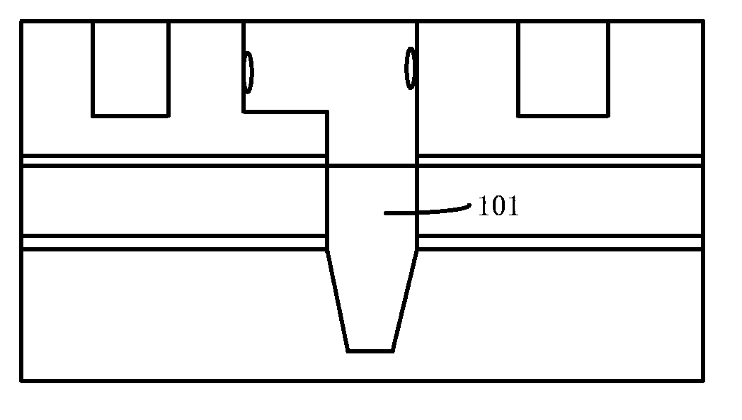
[0032] In order to thoroughly understand the present invention, a detailed description will be provided in the following description to illustrate the preparation method of the double damascene structure of the present invention. Obviously, the practice of the invention is not limited to specific details familiar to those skilled in the semiconductor arts. Preferred embodiments of the present invention are described in detail below, however, the present invention may have other embodiments besides these detailed descriptions.

[0033] It should be noted that t...


PUM

PropertyMeasurementUnit
thicknessaaaaaaaaaa
thicknessaaaaaaaaaa
thicknessaaaaaaaaaa

Abstract

The invention relates to a method for preparing a dual damascene structure. The method comprises the following steps: providing a semiconductor substrate; sequentially forming an etching stop layer, a dielectric layer, a hard mask laminated layer and a metallic hard mask layer on the substrate; etching the metallic hard mask layer and the hard mask laminated layer to form tapered openings; forming a patterned through hole mask layer on the metallic hard mask layer; etching the dielectric layer to form a plurality of grooves and through holes; filling the grooves and the through holes by a metallic material and executing chemical-mechanical planarization. In order to achieve a better effect when the through holes are filled, the tapered openings are first formed on the metallic hard mask layer, an oxide hard mask layer and a low-k material hard mask layer so as to obtain the openings with big tops, the through holes are filled through the tapered openings, a better filling effect can be achieved, and the problem in the prior art that holes and gaps easily occur is solved.

Description

technical field [0001] The invention relates to the field of semiconductors, in particular, the invention relates to a preparation method of a double damascene structure. Background technique [0002] With the continuous advancement of semiconductor integrated circuit process technology, when semiconductor devices are reduced to a deep sub-micron range, the resistance (R) and capacitance (C) in the interconnection are prone to parasitic effects, resulting in the time delay of metal connection transmission (RC time delay). In order to overcome the parasitic effect in interconnection, more and more people use low-resistance material (copper) or isolation material with low dielectric constant (low k dielectric) in the integration process of VLSI back-end interconnection to reduce RC delay time due to parasitic resistance and parasitic capacitance. However, when the material of the metal wire is changed from aluminum to copper with lower resistivity, since copper diffuses into...

Claims


Application Information

Patent Timeline
Patent Type & Authority Applications(China)
IPC IPC(8): H01L21/768
CPCH01L21/76804H01L21/76807H01L21/76814
Inventor 王新鹏胡敏达周俊卿
Owner SEMICON MFG INT (SHANGHAI) CORP
Why Eureka
Try Eureka