Planar vdmos transistor and its preparation method

A transistor and planar technology, which is applied in semiconductor/solid-state device manufacturing, semiconductor devices, electrical components, etc., can solve the problems of planar VDMOS transistor itself, high switching speed, electromagnetic interference of switching circuits, etc., to reduce electromagnetic interference, Effect of reducing electromagnetic interference and reducing on-resistance

Active Publication Date: 2017-07-14
WUXI CHINA RESOURCES HUAJING MICROELECTRONICS
View PDF1 Cites 0 Cited by
  • Summary
  • Abstract
  • Description
  • Claims
  • Application Information

AI Technical Summary

Problems solved by technology

However, the applicant found that if the loss of the planar VDMOS transistor is too high and the switching speed is too fast, it is easy to cause electromagnetic interference problems in the switching circuit

Method used


Image

  • Planar vdmos transistor and its preparation method
  • Planar vdmos transistor and its preparation method
  • Planar vdmos transistor and its preparation method

Examples


Embodiment Construction

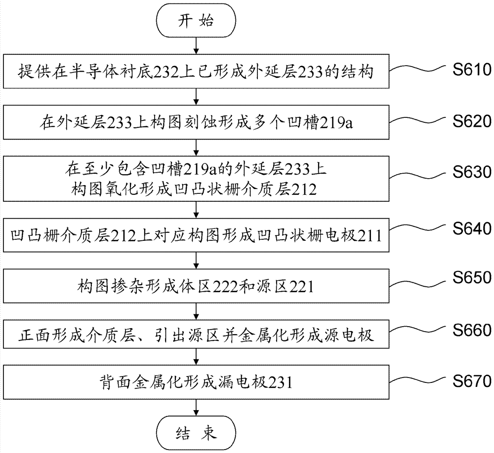
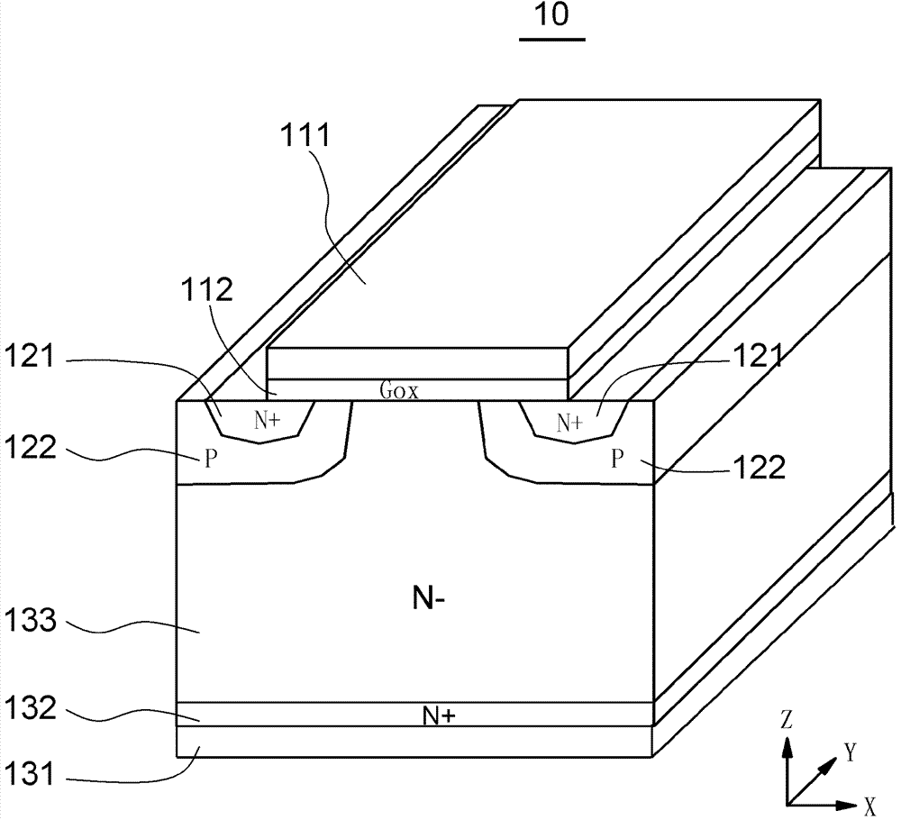
[0032] The following introduces some of the possible embodiments of the present invention, which are intended to provide a basic understanding of the present invention, but are not intended to identify key or decisive elements of the present invention or limit the scope of protection. It is easy to understand that, according to the technical solution of the present invention, those skilled in the art may propose other alternative implementation manners without changing the essence and spirit of the present invention. Therefore, the following specific embodiments and drawings are only exemplary descriptions of the technical solution of the present invention, and should not be regarded as the entirety of the present invention or as a limitation or restriction on the technical solution of the present invention.

[0033] In the drawings, the thicknesses of layers and regions are exaggerated for clarity, and shape features such as roundness caused by manufacturing processes such as ...


PUM


Abstract

The invention provides a planar VDMOS (Vertical Double-Diffusion Metal-Oxide-Semiconductor) transistor and a preparation method thereof and belongs to the field of VDMOS transistor devices. The planar VDMOS transistor comprises a substrate, an epitaxial layer, a body region, a source region, a gate dielectric layer and a gate electrode, wherein the epitaxial layer is formed on the substrate, the body region and the source region are formed in the epitaxial layer, and the gate dielectric layer is formed on the epitaxial layer. One or more grooves basically parallel to the channel direction of the planar VDMOS transistor are formed in the upper surface of part, of the epitaxial layer, corresponding to the gate dielectric layer, and the corresponding part, of the gate dielectric layer, above the grooves is correspondingly sunken to form a concave-convex gate dielectric layer. The planar VDMOS transistor has the characteristics of small on resistance, and small loss and no electromagnetic interference during switching application.

Description

technical field [0001] The invention belongs to the field of VDMOS (Vertical Double-diffused Metal-Oxide-Semiconductor, vertical double-diffused metal-oxide-semiconductor) transistor devices, and relates to a planar VDMOS transistor with a concave-convex gate dielectric layer and a preparation method thereof. Background technique [0002] DMOS (Double-diffused Metal-Oxide-Semiconductor, double-diffused metal-oxide-semiconductor) transistor is a kind of MOSFET, which has the characteristics of high power and high breakdown voltage, and is one of the common power devices. Generally, according to the orientation of the drift region in DMOS relative to the substrate surface, it can be divided into lateral DMOS (LDMOS) and VDMOS transistors; VDMOS transistors further include trench VDMOS transistors and planar VDMOS transistors. [0003] figure 1 Shown is a schematic diagram of a three-dimensional cell structure of a traditional planar VDMOS transistor. Such as figure 1 As sho...

Claims


Application Information

Patent Timeline
Patent Type & Authority Patents(China)
IPC IPC(8): H01L29/78H01L29/423H01L29/06H01L21/336
CPCH01L29/0603H01L29/42368H01L29/66712H01L29/7802
Inventor 唐红祥张新彭强
Owner WUXI CHINA RESOURCES HUAJING MICROELECTRONICS
Why Eureka
Try Eureka