Method for preparing planar sample for transmission electron microscope at specific failure point

An electron microscope and plane sample technology, applied in the field of semiconductors, can solve the problems of being difficult to grasp, being ground, and the method of manual grinding is difficult to control accurately, so as to achieve the effect of improving the success rate

Active Publication Date: 2014-04-02
WUHAN XINXIN SEMICON MFG CO LTD
View PDF5 Cites 9 Cited by
  • Summary
  • Abstract
  • Description
  • Claims
  • Application Information

AI Technical Summary

Problems solved by technology

There are problems with this method: it is difficult to control precisely by manual grinding, and it is difficult to grind a section of a silicon wafer to a distance of 1-2 microns from a specific failure point, and it is easy to be ground.

Method used


Image

  • Method for preparing planar sample for transmission electron microscope at specific failure point
  • Method for preparing planar sample for transmission electron microscope at specific failure point
  • Method for preparing planar sample for transmission electron microscope at specific failure point

Examples


Embodiment Construction

[0026] The principles and features of the present invention are described below in conjunction with the accompanying drawings, and the examples given are only used to explain the present invention, and are not intended to limit the scope of the present invention.

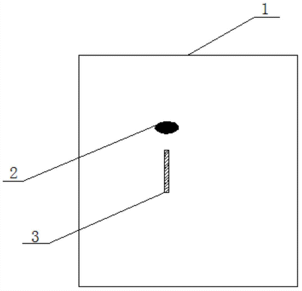
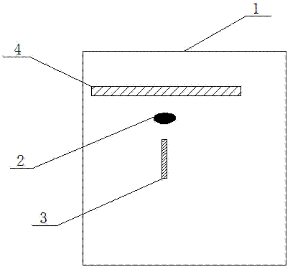
[0027] Such as Figure 1 to Figure 6 As shown, a method of preparing a planar sample for transmission electron microscopy at a specific point of failure, including:

[0028] Step 1, place the silicon wafer 1 with the specific failure point 2 horizontally on the sample stage 7 of the focused ion beam machine, make a specific failure point mark 3 on the silicon wafer 1, and make a specific failure point mark 3 on the silicon wafer 1 2 for positioning. Specifically, a rectangular specific failure point mark 3 is formed by bombarding with a focused ion beam.

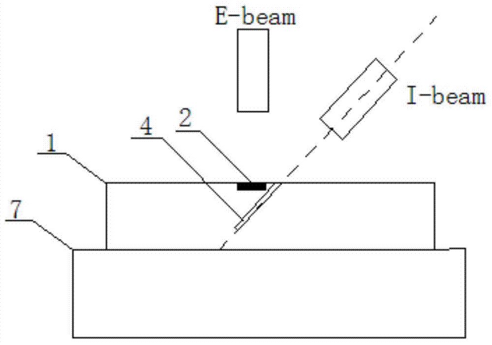
[0029] Step 2, adjust the angle of the sample stage 7 so that the silicon wafer 1 is not perpendicular to the focused ion beam; the angle between the focused io...


PUM


Abstract

The invention discloses a method for preparing a planar sample for a transmission electron microscope at a specific failure point. The method comprises the following steps: intercepting a piece of the sample close to the failure point on the sample by a focused ion beam, sucking the intercepted sample by a Pick-Up system and vertically placing the intercepted sample on the surface of a silicon slice, and fixing the sample on the surface of the silicon slice by means of focused ion beam gold-plating to prepare the planar sample for the transmission electron microscope. According to the method disclosed by the invention, by accurately intercepting the sample by the focused ion beam, a process of manually grinding is omitted, the success rate of sample preparation and the quality of the sample are greatly improved, and great assistance is provided for the subsequent failure analysis and structure analysis.

Description

technical field [0001] The invention relates to the technical field of semiconductors, in particular to a method for preparing a transmission electron microscope plane sample at a specific failure point. Background technique [0002] Transmission Electron Microscope (TEM) is a large-scale microscopic analysis equipment that uses high-energy electron beams as illumination sources for magnified imaging. At present, the conventional method used to prepare TEM flat samples at specific failure points is: first In the focused ion beam machine, use the focused ion beam etching method to mark near the specific failure point that needs to be observed, and then use manual grinding to grind a section of the silicon wafer to about 1-2 microns away from the specific failure point. Finally, put it vertically into the focused ion beam machine to prepare the transmission electron microscope sample. There are problems with this method: it is difficult to control precisely by manual grinding...

Claims


Application Information

Patent Timeline
Patent Type & Authority Applications(China)
IPC IPC(8): G01N1/28
Inventor 李剑郭伟仝金雨李桂花
Owner WUHAN XINXIN SEMICON MFG CO LTD
Why Eureka
Try Eureka