
Semiconductor gas sensor

A gas sensor and semiconductor technology, used in instruments, scientific instruments, measuring devices, etc., can solve the problems of high cost, different regional temperatures, and high power consumption, achieve uniform thermal field, reduce surface power loss, and reduce power consumption. consumption effect

Active Publication Date: 2014-04-02
SUZHOU NANOGRID TECH
View PDF9 Cites 7 Cited by
  • Summary
  • Abstract
  • Description
  • Claims
  • Application Information

AI Technical Summary

Problems solved by technology

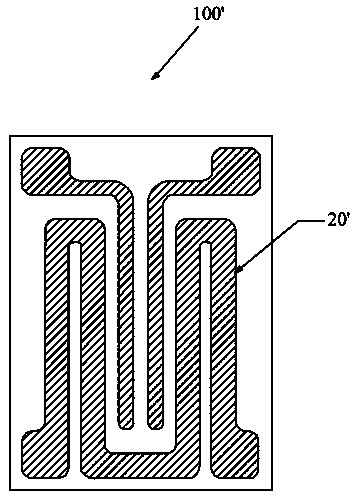
[0004] At present, when gas sensors are prepared by microelectronics technology, most of the gas sensors in the prior art have relatively large power consumption and are not energy-saving, or use expensive materials to complete low power consumption, but the cost is relatively high; The bottom of the substrate is etched into an inverted pyramid-shaped pit to reduce power consumption. However, although the sensor with this structure has low power consumption, the preparation process requires multiple photolithography processes, etching processes, and deposition processes. The process flow It is more complicated and the cost is higher; in addition, the temperature of the heating electrode on the surface of the substrate is not uniform, and the regional temperature is different

Method used


Image

  • Semiconductor gas sensor
  • Semiconductor gas sensor
  • Semiconductor gas sensor

Examples


Embodiment Construction

[0033] The present invention will be described in detail below in conjunction with specific embodiments shown in the accompanying drawings. However, these embodiments do not limit the present invention, and any structural, method, or functional changes made by those skilled in the art according to these embodiments are included in the protection scope of the present invention.

[0034] It should be noted that in different implementations / embodiments, the same symbols or signs may be used, but this does not represent the same or connection in structure, but is only for the convenience of description.

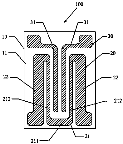
[0035] ginseng figure 1 , to introduce a specific embodiment of the semiconductor gas sensor 100 of the present invention, the semiconductor gas sensor 100 includes a substrate 10 , a signal sensing electrode 30 , and a heating electrode 20 .

[0036] The substrate 10 has a surface 11, which is relatively determined for subsequent circuit layout, the heating electrode 20 is fabr...


PUM


Abstract

The invention discloses a semiconductor gas sensor, comprising a base, a heating electrode, and a signal sensing electrode, wherein the base comprises a surface; the heating electrode is arranged on the surface; the signal sensing electrode is arranged inside a heat field formed by the heating electrode; the heating electrode is insulated with the signal sensing electrode; the heating electrode comprises a primary heating section and a secondary heating section; the primary heating section is adjacent to the signal sensing electrode; the secondary heating section is relatively far away from the signal sensing electrode; the resistance of the main heating section is greater than that of the secondary heating section. By adopting the semiconductor gas sensor disclosed by the invention, more effective utilization of the heat generated by the heating electrode is ensured by setting the primary heating section near the signal sensing electrode in the heating electrode to have the resistance greater than that of the secondary heating section which is relatively far away from the signal sensing electrode, and the surface power loss is reduced. Thus, power consumption of the sensor is reduced.

Description

technical field [0001] The invention belongs to the technical field of electronic device manufacturing, and in particular relates to a semiconductor gas sensor. Background technique [0002] With the development of society and the advancement of science and technology, the scale of industrial production has gradually expanded, but the resulting accidents have also occurred continuously, such as the flammable, explosive, toxic and harmful gases produced by the petrochemical and coal mining industries. Once these gases exceed the standard, Leakage will seriously affect the health of production personnel and surrounding residents, and if an explosion occurs, it will cause casualties and property losses. In addition, with the improvement of people's living standards and the change of people's requirements for home environment decoration, the problem of indoor air quality has become increasingly prominent, and malignant cases caused by excessive toxicity after decoration have bee...

Claims


Application Information

Patent Timeline
Patent Type & Authority Applications(China)
IPC IPC(8): G01N27/00
Inventor 张克栋徐红艳崔铮
Owner SUZHOU NANOGRID TECH
Learn More