Chip packaging structure with cavity and packaging method thereof

A technology of chip packaging structure and packaging method, which is applied in the fields of electric solid-state devices, semiconductor devices, semiconductor/solid-state device manufacturing, etc., can solve the problems of unsatisfactory performance requirements and reliability, heat dissipation and power distribution, etc., and achieve excellent heat dissipation and production The process is simple and advanced, and the effect of improving reliability

Active Publication Date: 2014-04-02
北京必创科技股份有限公司
View PDF4 Cites 5 Cited by
  • Summary
  • Abstract
  • Description
  • Claims
  • Application Information

AI Technical Summary

Problems solved by technology

Although the microelectronic packaging in the prior art provides protection to the chip in terms of electrical, thermal, optical and mechanical properties, it cannot

Method used


Image

  • Chip packaging structure with cavity and packaging method thereof
  • Chip packaging structure with cavity and packaging method thereof
  • Chip packaging structure with cavity and packaging method thereof

Examples


Embodiment 1

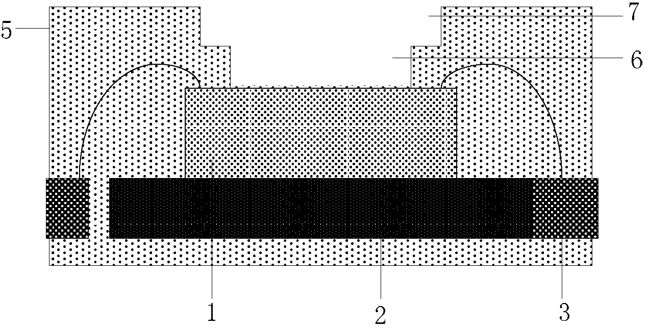
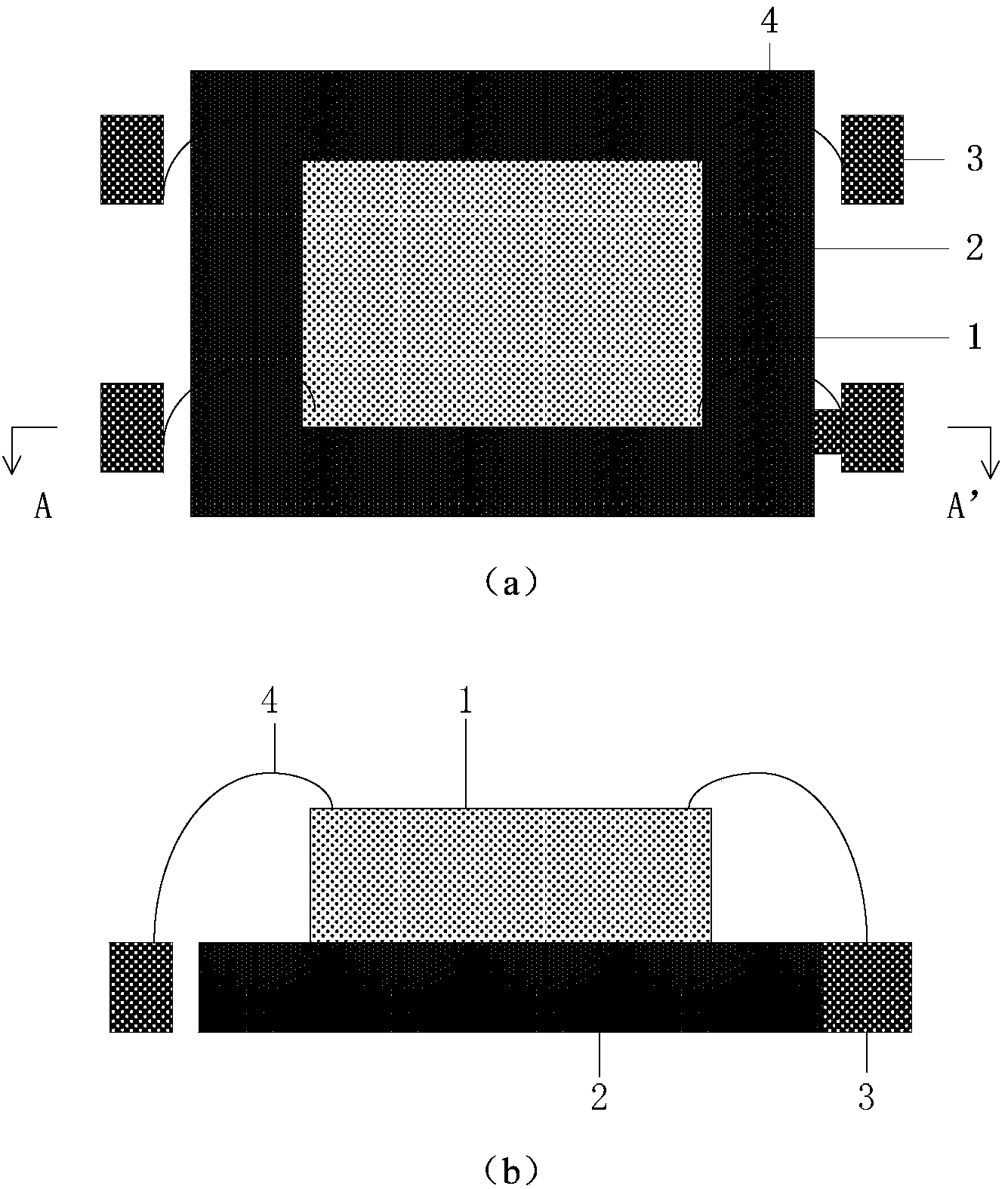
[0034] Such as figure 1 As shown, the chip packaging structure of the present embodiment includes: a chip 1, a substrate 2, a lead frame 3, a wire 4 and a plastic package 5; wherein, the lower surface of the chip 1 is pasted on the substrate 2; The foot frame 3 is connected; the plastic package body 5 packages the chip 1, the lead frame 3 and the substrate 2, and exposes the lead frame 3 on the side of the plastic package body 5; the upper surface of the chip is provided with a stress structure, and the plastic package body 5 and the chip 1 A cavity 6 is opened on the corresponding part of the upper surface, so that the upper surface of the chip is not in contact with the plastic package; and a through hole 7 is opened between the cavity 6 and the upper surface of the plastic package 5, so that the upper surface of the chip is not covered by the plastic package , to ensure that the stress of the chip is not affected, and it is connected with the outside world, which is conduci...

Embodiment 2

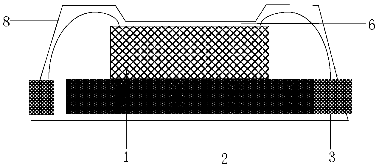
[0043] The chip packaging structure of this embodiment includes: chip 1, substrate 2, lead frame 3, lead 4, plastic package body 5 and sealing film 8; Wherein, the lower surface of chip 1 is pasted on the substrate 2; The lead frame 3 is connected; the sealing film 8 wraps the chip, the lead frame and the substrate, and exposes the bottom surface or side of the lead frame, and seals the sealing film and the edge of the lead frame, thereby forming a cavity between the plastic package and the chip 6, such as image 3 As shown; the plastic package is packaged outside the sealing film, and the lead frame that is not wrapped by the sealing film is exposed on the bottom surface or side of the plastic package; there is a through hole 7 between the plastic package 5 and the sealing film 8 corresponding to the sensitive part, Such as Figure 4 shown.

[0044]In this embodiment, the plastic package body 5 is made of epoxy resin; the sealing film 8 is made of polyester film, the cost i...


PUM


Abstract

The invention discloses a chip packaging structure with a cavity and a packaging method thereof. The chip packaging structure comprises a chip, a substrate, a pin frame, a wire and a plastic package body, wherein the lower surface of the chip is arranged on the substrate; the chip is connected with the pin frame by the wire; the plastic package body is used for packaging the chip, the pin frame and the substrate; the pin frame is exposed out of the bottom surface or the side face of the plastic package body; the cavity is arranged between the plastic package body and the chip, so that one surface which does not contact with the plastic package body at least exists in the side face and the upper surface of the chip. The cavity is arranged between the plastic package body and the chip, so the sensitive part of the surface of the chip does not contact with the plastic package body, the sensitive part is not covered by the plastic package body, and the stress influence on the internal structure of the chip, which is caused by the packaging structure is reduced; the chip packaging structure further comprises a through hole which is beneficial for the ventilation and the heat radiation of the chip; the packaging structure has the characteristics that the manufacturing process is simple and advanced, the size is relatively small, the heat radiation is excellent and the like, and the reliability in the using process of the electronic chip is improved.

Description

technical field [0001] The invention relates to semiconductor packaging technology, in particular to a chip packaging structure with a cavity and a packaging method thereof. Background technique [0002] In today's consumer electronics, automotive electronics, and the more demanding aviation, aerospace, and military industries, the requirements for electronic chips and other products with features such as multi-function, high performance, miniaturization, light weight, portability, and low cost are increasing. come higher. Packaging these chips with I / O pins to make electronic products that meet various uses and requirements requires wafer-level chip-scale packaging (WL-CSP), multi-chip module (MCM) or three-dimensional system-level Packaging module (3D SiP module) and other modern microelectronic packaging technologies. The rapid development of modern microelectronic packaging technology is constantly changing people's work and lifestyle, and prompting the whole world to ...

Claims


Application Information

Patent Timeline
IPC IPC(8): H01L23/31H01L23/367H01L21/50H01L21/56
CPCH01L2924/0002H01L2924/1815H01L2224/48091H01L2224/48247H01L2924/00014
Inventor 周浩楠张威苏卫国李宋陈广忠詹清颖张亚婷
Owner 北京必创科技股份有限公司
Why Eureka
Try Eureka