Image sensor and forming method thereof

An image sensor, tensile stress technology, applied in the direction of electric solid devices, semiconductor devices, electrical components, etc., can solve the problems affecting the performance of semiconductor devices, increase in interface trap density, etc., to improve interface trap density, improve speed performance, and improve motion. effect of speed

Inactive Publication Date: 2018-07-13
HUAIAN IMAGING DEVICE MFGR CORP
View PDF4 Cites 7 Cited by
  • Summary
  • Abstract
  • Description
  • Claims
  • Application Information

AI Technical Summary

Problems solved by technology

However, both titanium nitride and tungsten will produce high mechanical stress on the semiconductor substrate, such as compressive stress (Compressive Stress), which may lead to a decre

Method used


Image

  • Image sensor and forming method thereof
  • Image sensor and forming method thereof
  • Image sensor and forming method thereof

Examples


Embodiment Construction

[0034] In the prior art, deep trench isolation is used to potentially suppress blooming and suppress optical crosstalk. The deep trench isolation usually uses a titanium nitride film as a filling material, or a stacked structure of titanium nitride and tungsten as a filling material.

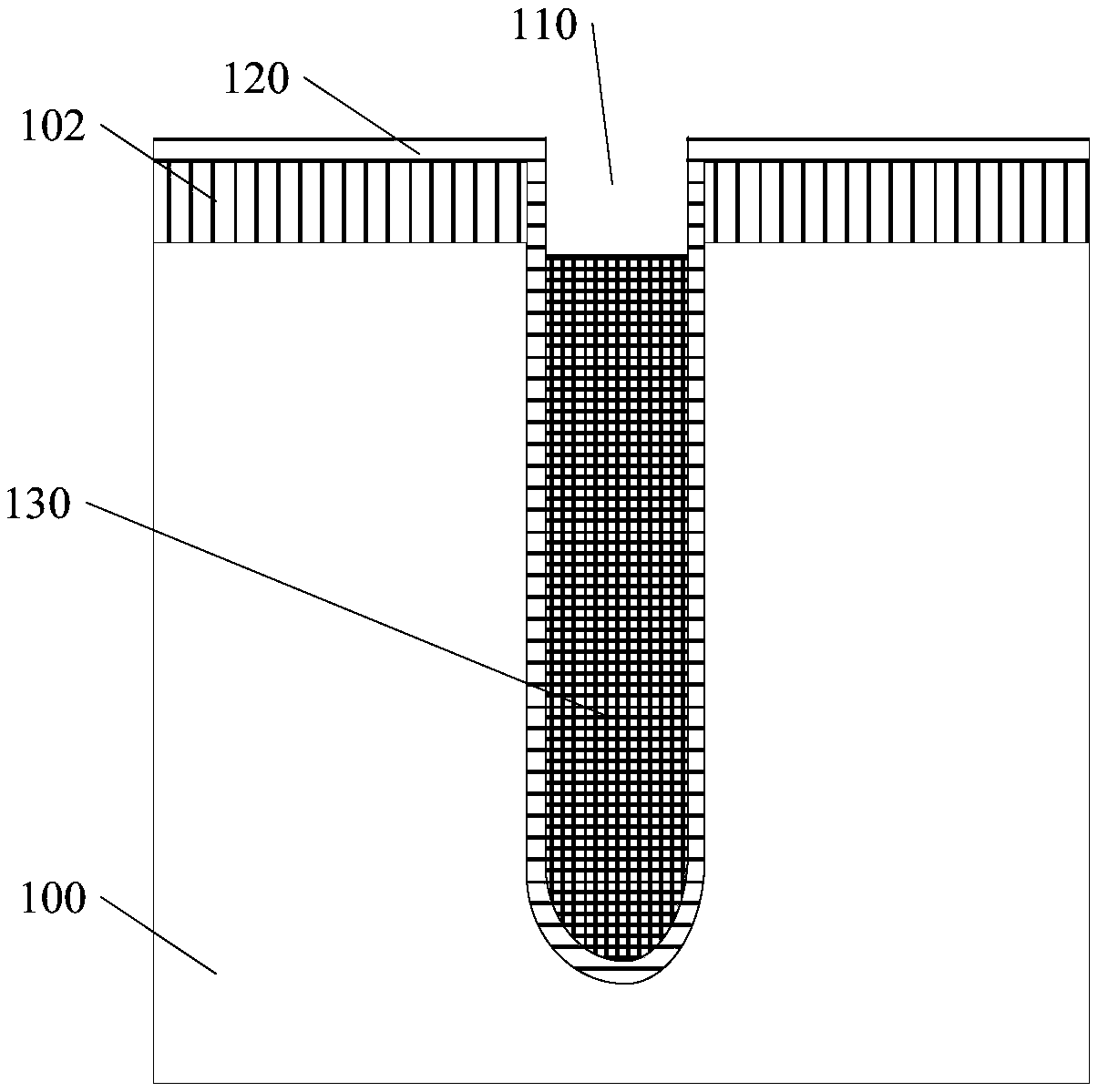
[0035] refer to figure 1 , figure 1 It is a schematic cross-sectional structure diagram of an image sensor in the prior art. The image sensor may include a semiconductor substrate 100 , a protective layer 102 , an isolation trench 110 , a dielectric film 120 and an alloy material layer 130 .

[0036] Specifically, a protective layer 102 is formed on the surface of the semiconductor substrate 100, and then a patterned mask layer is formed on the surface of the protective layer 102. Using the patterned mask layer as a mask, the protective layer 102 and the semiconductor substrate 100 are etched to form the isolation trench 110 .

[0037] Further, a dielectric film 120 is formed in the isolatio...


PUM


Abstract

The invention discloses an image sensor and a forming method thereof. The forming method includes: providing a semiconductor substrate; etching the semiconductor substrate to form an isolating groove;forming a medium thin film which covers the inner wall of the isolating groove; forming a metal blocking layer which covers the medium thin film; forming a tensile stress layer which fills at least apart of groove space surrounded by the metal blocking layer. By the forming method, compressive stress generated on the semiconductor substrate by a filling material in deep-groove isolation can be lowered.

Description

technical field [0001] The invention relates to the field of semiconductor manufacturing, in particular to an image sensor and a forming method thereof. Background technique [0002] The image sensor is the core component of the camera equipment, which realizes the image capture function by converting the optical signal into an electrical signal. Taking CMOS Image Sensors (CIS) devices as an example, in the manufacturing process, in order to prevent the photogenerated carriers in different regions from diffusing to adjacent regions, it is necessary to form Deep Trench Isolation (Deep Trench Isolation, DTI). [0003] Specifically, deep trench isolation can potentially suppress blooming, and for Back-side Illumination (BSI) CIS, metal material is used to fill the isolation trench to form deep trench isolation, which can suppress optical crosstalk. Wherein, the back-illuminated CIS may also be referred to as a back-illuminated CIS. [0004] In the prior art, a titanium nitri...

Claims


Application Information

Patent Timeline
IPC IPC(8): H01L27/146
CPCH01L27/1463H01L27/14636H01L27/14685
Inventor 鯨井裕
Owner HUAIAN IMAGING DEVICE MFGR CORP
Why Eureka
Try Eureka