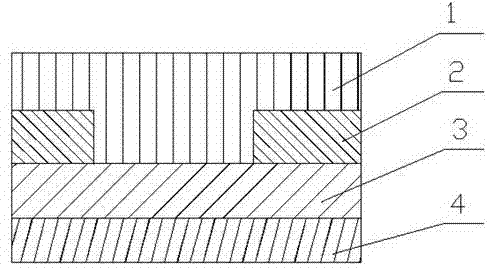
Method for manufacturing OGS (one glass solution) touch screen by means of electroplating BM (black matrix) on front surface thereof
A touch screen, single-touch technology, applied in electrical digital data processing, data processing input/output process, instruments, etc., can solve the problems of high cost, complex structure, low yield rate, etc.
- Summary
- Abstract
- Description
- Claims
- Application Information
AI Technical Summary
Problems solved by technology
Method used
Image
Examples
Embodiment 1
[0009] Prepare a glass substrate with a thickness of 0.2mm, and perform chemical strengthening treatment on it to enhance the strength of the glass substrate; (2) Coat a layer of ITO film with a thickness of 100mm on the lower surface of the glass substrate. A capacitive sensing structure composed of transparent conductive patterns on the lower surface is set in the touch ITO film layer, and a touch sensing layer pattern is made; (3) A BM layer with a thickness of 0.3um is electroplated on one side of the upper surface of the glass substrate, and customized (4) Coating a transparent layer with a thickness of 0.1um on one side of the upper surface of the BM layer, and doing customized anti-scratch treatment, anti-fingerprint treatment, and gap treatment; The ultra-thin front of the ultra-thin mobile phone is plated with BM's OGS touch screen.
Embodiment 2
[0011] Prepare a glass substrate with a thickness of 1.1mm, and perform chemical strengthening treatment on it to enhance the strength of the glass substrate; (2) Coat a layer of ITO film with a thickness of 300 μm on the lower surface of the glass substrate. A capacitive sensing structure composed of transparent conductive patterns on the lower surface is set in the touch ITO film layer, and a touch sensing layer pattern is made; (3) A BM layer with a thickness of 1.5um is plated on one side of the upper surface of the glass substrate and customized (4) Coating a transparent layer with a thickness of 1mm on one side of the upper surface of the BM layer, and doing customized anti-scratch treatment, anti-fingerprint treatment, and gap treatment; thus, the front electroplated BM The OGS touch screen can be used to touch the display screen of a computer.
Embodiment 3
[0013] Prepare a glass substrate with a thickness of 0.5mm, and perform chemical strengthening treatment on it to enhance the strength of the glass substrate; (2) Coat a layer of ITO film with a thickness of 200 µm on the lower surface of the glass substrate. A capacitive sensing structure composed of transparent conductive patterns on the lower surface is set in the touch ITO film layer, and a touch sensing layer pattern is made; (3) A BM layer with a thickness of 0.7um is plated on one side of the upper surface of the glass substrate and customized (4) Coating a transparent layer with a thickness of 0.5um on one side of the upper surface of the BM layer, and doing customized anti-scratch treatment, anti-fingerprint treatment, and gap treatment; BM's OGS touch screen can be used in mobile phones, tablets, navigators, etc.
PUM
| Property | Measurement | Unit |
|---|---|---|
| Thickness | aaaaa | aaaaa |
| Thickness | aaaaa | aaaaa |
| Thickness | aaaaa | aaaaa |
Abstract
Description
Claims
Application Information
 - R&D
- Intellectual Property
- Life Sciences
- Materials
- Tech Scout
- Unparalleled Data Quality
- Higher Quality Content
- 60% Fewer Hallucinations
Browse by: Latest US Patents, China's latest patents, Technical Efficacy Thesaurus, Application Domain, Technology Topic, Popular Technical Reports.
© 2025 PatSnap. All rights reserved.Legal|Privacy policy|Modern Slavery Act Transparency Statement|Sitemap|About US| Contact US: help@patsnap.com

