

A Broadband Absorbing Material Based on Subwavelength Metallic Structure
A metal structure and wave absorbing material technology, applied in electrical components, magnetic field/electric field shielding, antennas, etc., can solve the problems of weak absorption, large quality, narrow absorption frequency band, etc., achieve strong absorption, simple production, increase wave absorption The effect of bandwidth
- Summary
- Abstract
- Description
- Claims
- Application Information
AI Technical Summary
Problems solved by technology
Method used
Image

Examples
Embodiment Construction
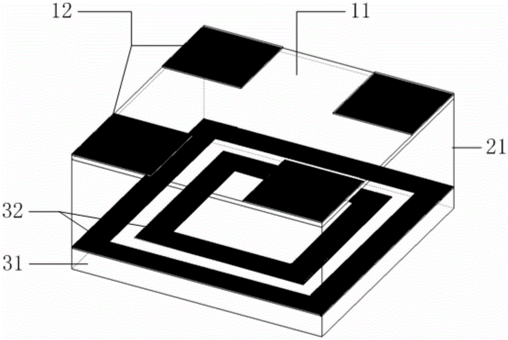
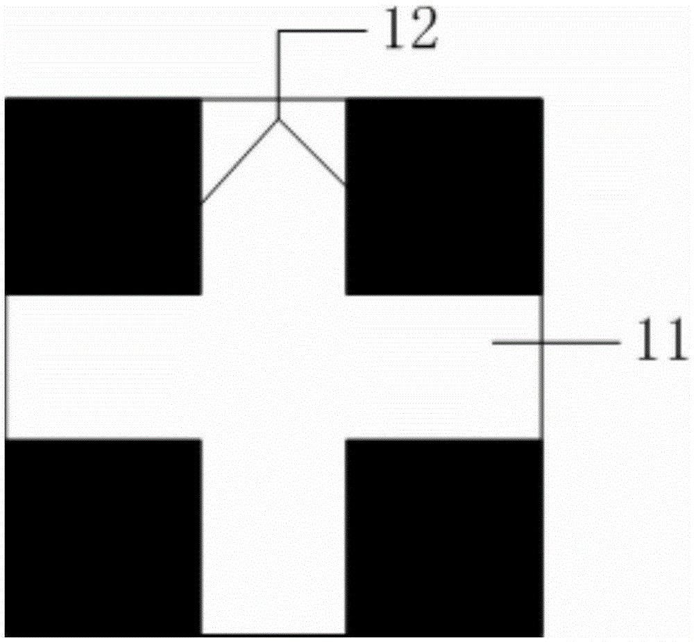
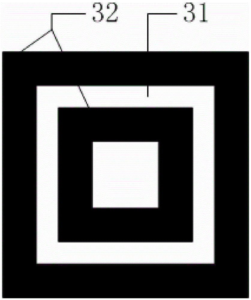
[0025] In the present invention, dielectric substrates coated with subwavelength metal structures of different shapes are respectively bonded on the upper and lower surfaces of traditional absorbing materials to form a three-layer structure. The upper surface of the first substrate is covered with periodically arranged rectangular metal structures; the second substrate is a sheet of traditional wave-absorbing material; the upper surface of the third substrate is covered with periodically arranged "back" Zigzag-shaped metal structure; every four rectangular metal structures on the first base material and one "back"-shaped metal structure on the third base material form a periodic unit, and the second base material is separated therebetween.
[0026] Both the first base material and the third base material are FR-4 materials, and the dielectric constant is ε=4.0-4.5.
[0027] The thickness of the first substrate is 0.127mm, and the thickness of the third substrate is 0.4mm to 0....
PUM
| Property | Measurement | Unit |
|---|---|---|
| thickness | aaaaa | aaaaa |
| thickness | aaaaa | aaaaa |
| thickness | aaaaa | aaaaa |
Abstract
Description
Claims
Application Information