Wave absorbing material
A wave-absorbing material and branching technology, applied in the field of materials, can solve the problems of limited mechanical properties of materials, lack of large-scale promotion, and unsatisfactory problems, and achieve the effect of thin thickness, simple structure, and high-efficiency electromagnetic waves
- Summary
- Abstract
- Description
- Claims
- Application Information
AI Technical Summary
Problems solved by technology
Method used
Image


Examples
Embodiment Construction
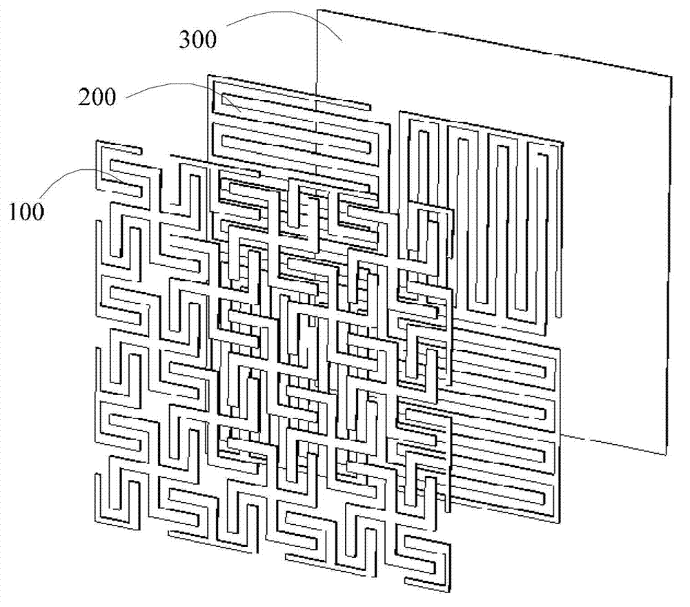
[0024] Please refer to figure 1 , figure 1 It is a schematic diagram of the structure of the absorbing material of the present invention. In the present invention, the first capacitive-resistance mixed layer 100 and the second capacitive-resistance mixed layer 200 are arranged in front of the target object to achieve broadband and high-efficiency absorption of electromagnetic waves. figure 1 Among them, the target object is represented by a metal sheet 300. In practical applications, the target object can be various objects with metal surfaces, such as airplanes, radars, etc. When the target object does not have a metal surface in practical applications, it can be placed on the surface of the target object Attach the metal layer.
[0025] In a preferred embodiment, the distance between the first capacitance-resistor mixture layer 100 and the second capacitance-resistance mixture layer 200 is equal to the distance between the second capacitance-resistance mixture layer 200 an...
PUM
 Abstract
Description
Claims
Application Information
 - R&D
- Intellectual Property
- Life Sciences
- Materials
- Tech Scout
- Unparalleled Data Quality
- Higher Quality Content
- 60% Fewer Hallucinations
Browse by: Latest US Patents, China's latest patents, Technical Efficacy Thesaurus, Application Domain, Technology Topic, Popular Technical Reports.
© 2025 PatSnap. All rights reserved.Legal|Privacy policy|Modern Slavery Act Transparency Statement|Sitemap|About US| Contact US: help@patsnap.com