SOI structure and manufacturing method thereof

A manufacturing method and substrate technology, which are applied in semiconductor/solid-state device manufacturing, electrical components, circuits, etc., can solve problems such as latch-up effect, and achieve the effect of reducing parasitic capacitance

Active Publication Date: 2014-04-16
SHANGHAI HUAHONG GRACE SEMICON MFG CORP
View PDF4 Cites 2 Cited by
  • Summary
  • Abstract
  • Description
  • Claims
  • Application Information

AI Technical Summary

Problems solved by technology

[0003] Semiconductor devices using bulk silicon substrates are prone to latch-up

Method used


Image

  • SOI structure and manufacturing method thereof
  • SOI structure and manufacturing method thereof
  • SOI structure and manufacturing method thereof

Examples


Embodiment Construction

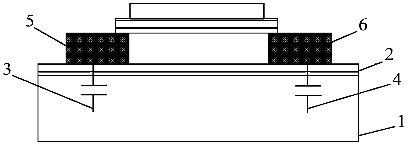
[0037] In the existing semiconductor device with SOI structure, a certain size of parasitic capacitance is easily generated between the source region, the drain region and the substrate, and the parasitic capacitance will affect the radio frequency characteristics of the semiconductor device, making the signal strength output by the device worse, The signal waveform is distorted.

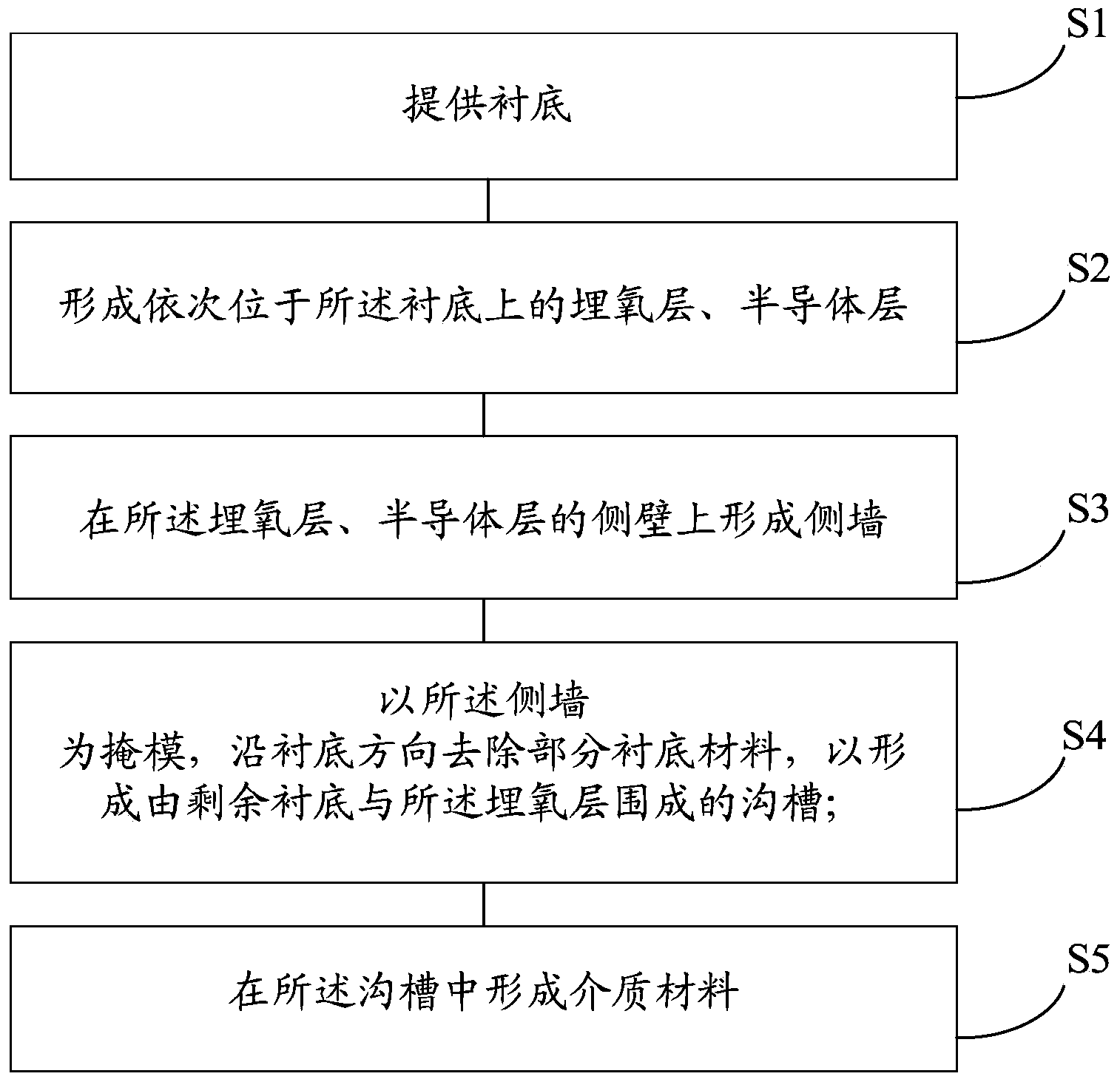
[0038] In order to solve the technical problem, the present invention provides an SOI structure, referring to figure 2 It is a schematic flow chart of an embodiment of the fabrication method of the SOI structure of the present invention. Described preparation method roughly comprises:

[0039] Step S1, providing a substrate;

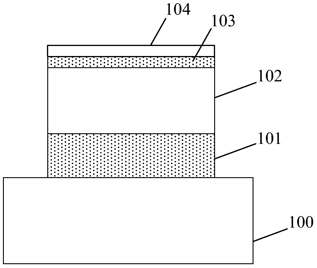
[0040] Step S2, forming a buried oxide layer and a semiconductor layer sequentially located on the substrate;

[0041] Step S3, forming sidewalls on the sidewalls of the buried oxide layer and the semiconductor layer;

[0042] Step S4, using the sidewall as a mask, removi...


PUM

PropertyMeasurementUnit
Thicknessaaaaaaaaaa

Abstract

A manufacturing method for an SOI structure comprises the steps of providing a substrate; forming a buried oxide layer and a semiconductor layer which are sequentially located on the substrate; forming side walls on the buried oxide layer and the semiconductor layer; with the side walls serving as masks, removing part of a substrate material in the substrate direction so as to form a groove encircled with the remaining substrate and the buried oxide layer; and forming a dielectric material in the groove. In addition, the invention further provides the SOI structure. The SOI structure comprises the substrate, the dielectric material located on the edge of the substrate, the buried oxide layer, the semiconductor layer and the side walls, wherein the buried oxide layer and the semiconductor layer are sequentially located on the substrate and the dielectric material, and the side walls are positioned on the buried oxide layer and the semiconductor layer. According to the technical scheme, the SOI structure and the manufacturing method have the advantages that the substrate is provided with the groove, the dielectric material is formed in the groove, the distance between the semiconductor layer and the substrate is increased, and parasitic capacitance between the semiconductor layer and the substrate is reduced.

Description

technical field [0001] The invention relates to the technical field of semiconductors, in particular to an SOI structure and a manufacturing method thereof. Background technique [0002] With the development of semiconductor technology, the integration level of integrated circuits is getting higher and higher, the feature size of devices is getting smaller and smaller, and the influence of devices themselves on radio frequency characteristics is becoming more and more obvious. [0003] Semiconductor devices using bulk silicon substrates are prone to latch-up effects. In the prior art, a silicon-on-insulator SOI (Silicon On Insulator, SOI) structure substrate has been developed, and a semiconductor device using the SOI structure has better radio frequency characteristics. [0004] refer to figure 1 , shows a schematic diagram of an SOI structure semiconductor device in the prior art. The semiconductor device includes: a substrate 1, a buried oxide layer 2 (Buried Oxide, BO...

Claims


Application Information

Patent Timeline
IPC IPC(8): H01L21/762H01L21/336H01L29/06H01L29/78
CPCH01L21/7624H01L29/0649H01L29/78
Inventor 刘张李
Owner SHANGHAI HUAHONG GRACE SEMICON MFG CORP
Why Eureka
Try Eureka