A threshold voltage adjustment method

A technology of threshold voltage and adjustment method, which is applied in the manufacture of circuits, electrical components, semiconductors/solid-state devices, etc.

Active Publication Date: 2016-04-06
FOUNDER MICROELECTRONICS INT
View PDF4 Cites 0 Cited by
  • Summary
  • Abstract
  • Description
  • Claims
  • Application Information

AI Technical Summary

Problems solved by technology

[0011] The embodiment of the present application provides a threshold voltage adjustment method, which can solve the technical problem that at least one photoresist layer needs to be added in the process of adjusting the threshold voltage of a high-voltage CMOS integrated circuit in the prior art

Method used


Image

  • A threshold voltage adjustment method
  • A threshold voltage adjustment method
  • A threshold voltage adjustment method

Examples


Embodiment Construction

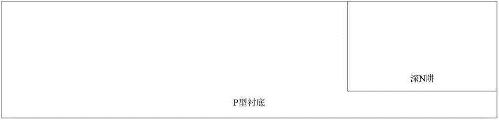
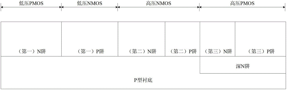
[0056] The embodiment of the application provides a threshold voltage adjustment method, which solves the need to add at least one photolithography layer in the deep N-well high-voltage CMOS integrated circuit manufacturing process to combine the four high-voltage NMOS, high-voltage PMOS, low-voltage NMOS, and low-voltage PMOS. The technical problem of adjusting the threshold voltage of the region to a predetermined range.

[0057] The technical solution of the embodiment of the present application is to solve the above-mentioned technical problem of adding at least one photolithography layer, and the general idea is as follows:

[0058] In the process of forming the first P-well, the second P-well, and the third P-well of the deep N-well high-voltage CMOS integrated circuit, implanting into the first P-well, the second P-well and the third P-well First ions that meet the first preset condition, the first ions are implanted twice to adjust the source-drain breakdown voltage and the...


PUM


Abstract

The invention discloses a threshold voltage adjusting method which is applied to a manufacturing process of a deep N-well high-voltage CMOS integrated circuit and can be used for adjusting threshold voltage of a high-voltage CMOS on the premise that a photoetching layer is not increased. The method includes the steps that when a first P well, a second P well and a third P well of the deep N-well high-voltage CMOS integrated circuit are formed, first ions according with first preset conditions are injected into the first P well, the second P well and the third P well, the first ions are injected in twice, and accordingly source drain breakdown voltage and threshold voltage of a high-voltage NMOS and source drain breakdown voltage and threshold voltage of a high-voltage PMOS are adjusted.

Description

Technical field [0001] The invention belongs to the field of semiconductor integrated circuit manufacturing, and particularly relates to a threshold voltage adjustment method. Background technique [0002] In the prior art, as the most basic electronic components, MOS tubes are commonly used in various electronic products. There are many types of MOS tubes, but they mainly include N-channel MOS tubes (NMOS) and P-channel MOS tubes (PMOS). [0003] In the high-voltage CMOS integrated circuit, four MOS transistors, low-voltage NMOS, low-voltage PMOS, high-voltage NMOS, and high-voltage PMOS, are integrated in the same chip. [0004] But no matter what kind of MOS tube, it is composed of well, source / drain region, gate oxide layer and polysilicon gate. Among them, NMOS tube is composed of P well, N+ source / drain region, gate oxide layer and polysilicon gate. PMOS tube It is composed of N well, P+ source / drain region, gate oxide layer and polysilicon gate. [0005] Several common parame...

Claims


Application Information

Patent Timeline
Patent Type & Authority Patents(China)
IPC IPC(8): H01L21/8238H01L21/265
CPCH01L21/823892
Inventor 潘光燃石金成高振杰林国胜王焜由云鹏
Owner FOUNDER MICROELECTRONICS INT
Why Eureka
Try Eureka