

Conductive pattern, method for forming the same, printed wiring board, and manufacturing method of the same
A conductive pattern and ink technology, applied in conductive pattern formation, printed circuit manufacturing, printed circuit, etc., can solve the problems of pattern fusion and inability to realize line image formation.
- Summary
- Abstract
- Description
- Claims
- Application Information
AI Technical Summary
Problems solved by technology
Method used
Image

Examples
Embodiment -
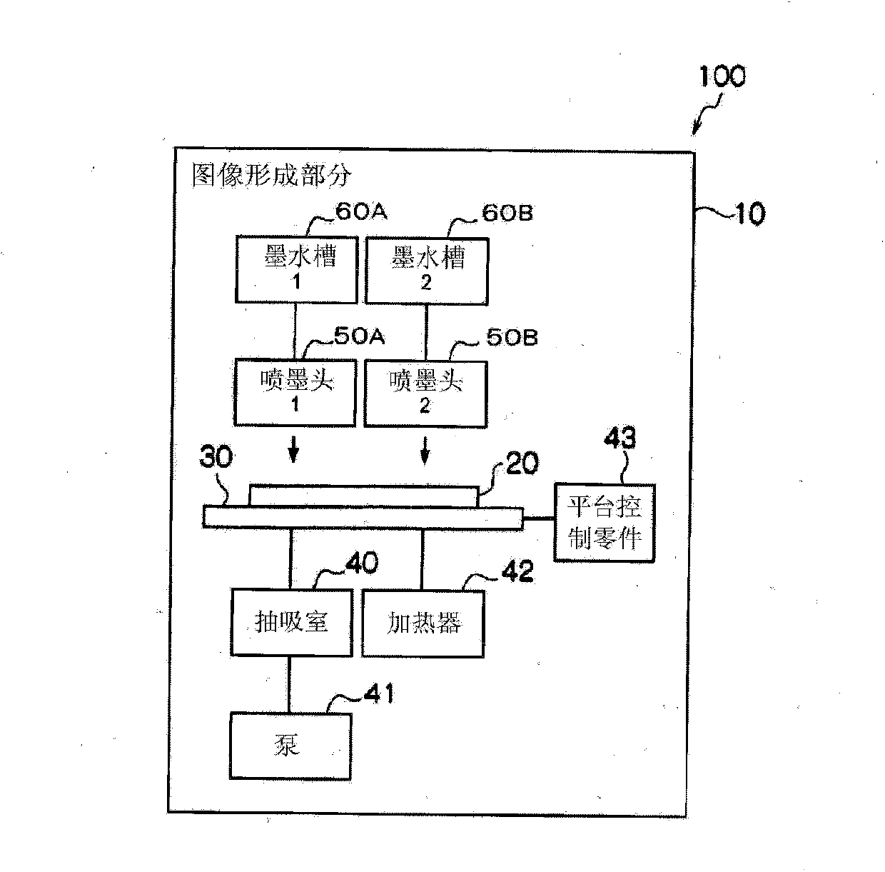
[0211] image 3 is an overall configuration view of the composition gradient layer manufacturing apparatus 100 according to the image forming hybrid method, and Figure 4 is a diagrammatic view of the image forming section 10 of the composition gradient layer manufacturing apparatus 100 . As shown in these figures, a composition gradient layer manufacturing apparatus 100 is configured to include an image forming section 10, and for the image forming section 10, a flat head type inkjet image forming apparatus is used. In detail, the image forming section 10 is configured to include a stage 30 on which the base material 20 is loaded; a suction chamber 40 for suctioning and fixing the base material 20 loaded on the stage 30; and an inkjet head 50A (hereinafter referred to as “inkjet head 1 ”) and inkjet head 50B (hereinafter referred to as “inkjet head 2 ”), each of which ejects each ink to base material 20 .
[0212] The platform 30 has a width dimension larger than the diamet...
example 1
[0297] (manufacturing inks containing curable compounds)
[0298] -Curable Ink A1-
[0299] N-vinylcaprolactam (manufactured by Sigma-Aldrich): 50 grams
[0300] Dipropylene glycol diacrylate (manufactured by Akcros Chemicals): 40 grams
[0301] Yanjiagu 184 (manufactured by Ciba Specialty Chemical Co., Ltd.): 4 grams
[0302] Lucillin TPO (manufactured by BASF AG): 6 grams
[0303] The above materials were charged into a 2 liter container and stirred for 20 minutes while maintaining the liquid temperature not higher than 40°C by a Silverson high speed stirrer. Subsequently, the resultant was filtered with a 2-micron filter to manufacture curable ink A1.
[0304] (Manufacturing Metallic Ink)
[0305] -Metallic ink B1-
[0306] Copper nanoparticles MD50 (average particle size: 50 nm, manufactured by Ishihara Sangyo Co., Ltd.
[0307] (manufactured by Ishihara Sangyo Kaisha, Ltd.): 10 g
[0308] Laurylamine (by Tokyo Chemical Industry Co., Ltd. (Tokyo Chemical Industry C...
example 2
[0337] As an ink of a mixture of curable ink A1 and metallic ink B1 used in Example 1, ink G1 (mixing ratio of A1 / B1 mass%=75 / 25), ink G2 (mixing ratio of A1 / B1 (mass%) =50 / 50) and ink G3 (mixing ratio (mass %) of A1 / B1=25 / 75). On a transparent PET base material (thickness: 150 µm, manufactured by Fujifilm Co., Ltd.), by the following inkjet image forming method B, a conductive film composed of a composition gradient layer with a thickness of 10 µm was formed by using five printing heads. A pattern (line width: 100 μm) in which the five above-mentioned inks also containing inks A1 and B1 have been filled in the order of A1 (lowermost layer), G1, G2, G3, and B1 (uppermost layer). By using the transparent PET base material on which the conductive pattern of the present invention was formed, the adhesion of the composition gradient layer to the base material, conductivity, and pattern formation were evaluated. The results are shown in Table 1 below.
[0338] -Inkjet image formi...
PUM
| Property | Measurement | Unit |
|---|---|---|
| boiling point | aaaaa | aaaaa |
| particle size | aaaaa | aaaaa |
| thickness | aaaaa | aaaaa |
Abstract
Description
Claims
Application Information