Method for increasing ITO (indium tin oxide) conductive film surface infrared band light transmittance

A conductive film, infrared band technology, applied in circuits, electrical components, semiconductor devices, etc., can solve the problems of weakening the ability to collect charges, increasing the resistance of ITO conductive films, uneven micro-nano structure, etc., to reduce uneven energy distribution. , The effect of improving power generation efficiency and improving power generation efficiency

Active Publication Date: 2014-04-23
XI AN JIAOTONG UNIV
View PDF5 Cites 4 Cited by
  • Summary
  • Abstract
  • Description
  • Claims
  • Application Information

AI Technical Summary

Problems solved by technology

For thin film materials such as ITO, when making large-area micro-nano structures, there will be uneven micro-nano structures, and even some ITO conductive films will be completely ablated under the irradiation of the center of the spot, making ITO conductive. The resistance of the film is greatly increased, which weakens its ability to collect charges, so it is very necessary to make a uniform large-area micro-nano structure on the surface of the ITO conductive film

Method used


Image

  • Method for increasing ITO (indium tin oxide) conductive film surface infrared band light transmittance
  • Method for increasing ITO (indium tin oxide) conductive film surface infrared band light transmittance
  • Method for increasing ITO (indium tin oxide) conductive film surface infrared band light transmittance

Examples


Embodiment 1

[0019] A method for improving the infrared band light transmittance on the surface of an ITO conductive film, comprising the following steps:

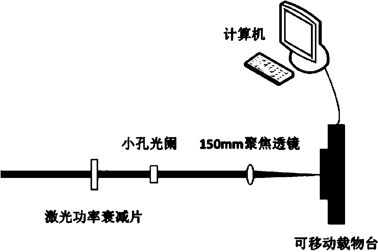
[0020] 1) First, adjust the picosecond laser output laser wavelength to 1064nm, repetition frequency 1KHz, pulse width 10ps, and adjust the laser power attenuator to stabilize the laser power at 25mw, such as figure 1 shown;

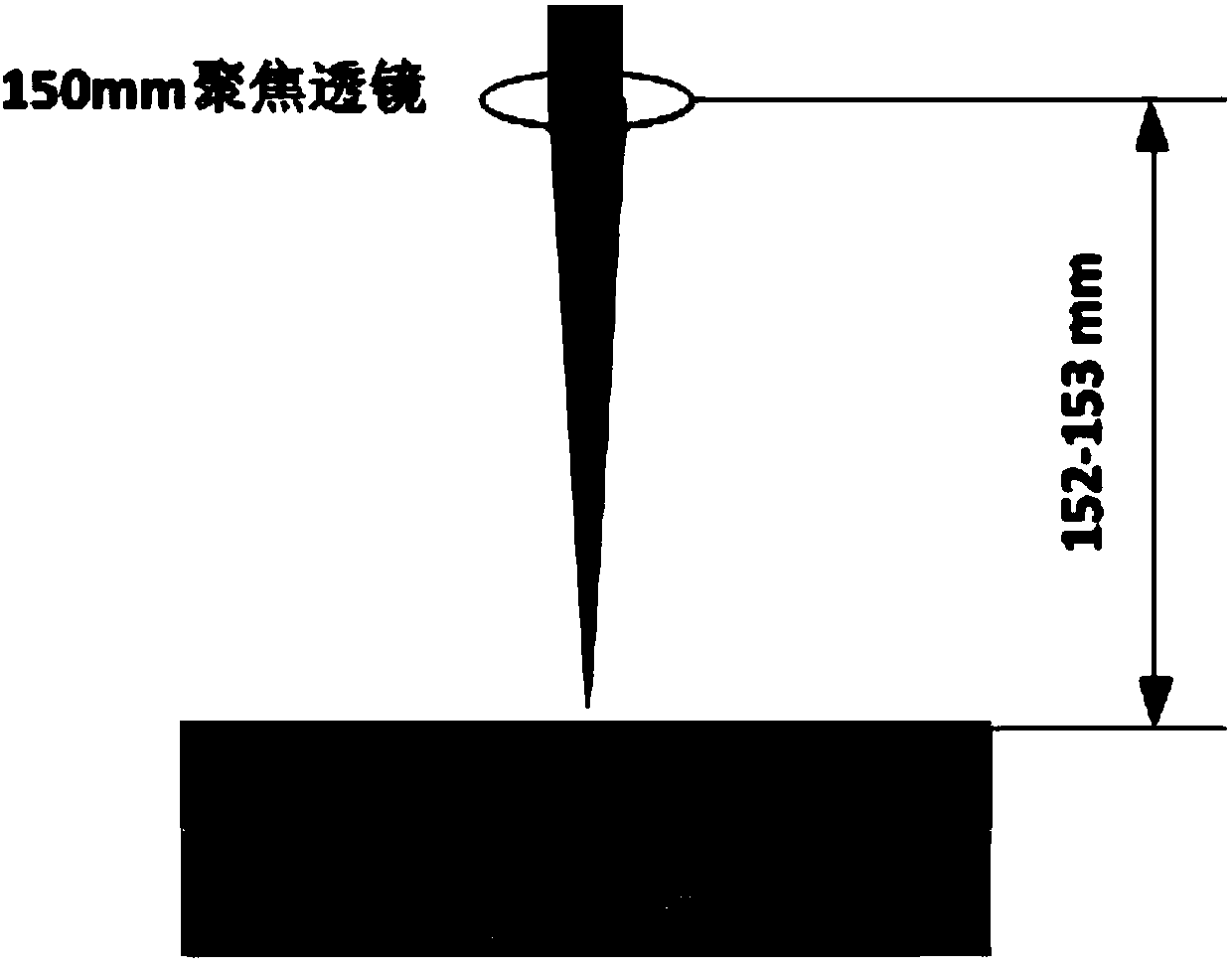
[0021] 2) Secondly, select a focusing lens with a focal length of 150mm in the optical path to focus the light beam, install a small aperture diaphragm in front of the focusing lens, and adjust the size of the aperture of the small aperture diaphragm so that the distance along the optical path is 2mm away from the focal point The spot size is 40μm, such as figure 1 shown;

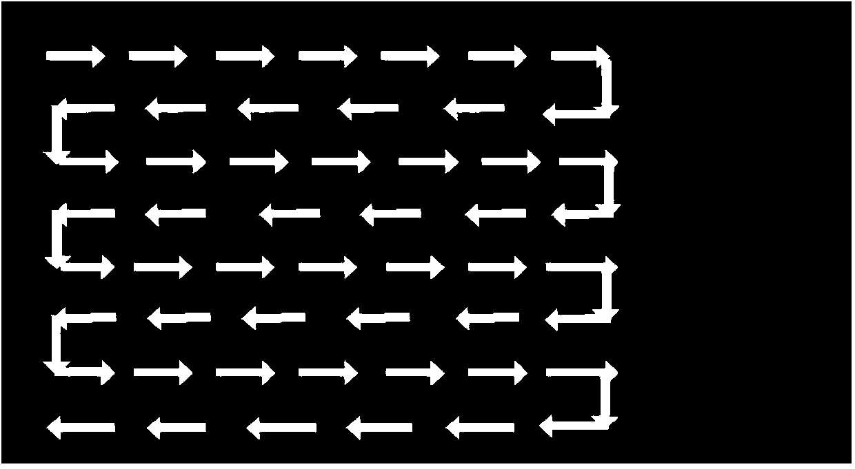
[0022] 3) Finally, use the adjusted picosecond laser to irradiate the ITO conductive film on the movable stage, and the movable stage moves in the horizontal direction at a speed of 2mm / s. When the laser spot reaches the horizontal direction...

Embodiment 2

[0024] A method for improving the infrared band light transmittance on the surface of an ITO conductive film, comprising the following steps:

[0025] 1) First, adjust the picosecond laser output laser wavelength to 1064nm, repetition frequency 1KHz, pulse width 10ps, adjust the laser power attenuator to stabilize the laser power at 22mw, such as figure 1 shown;

[0026] 2) Secondly, select a focusing lens with a focal length of 150mm in the optical path to focus the light beam, install a small aperture diaphragm in front of the focusing lens, and adjust the size of the aperture of the small aperture diaphragm so that the distance along the optical path is 2mm away from the focal point The spot size is 45μm, such as figure 1 shown;

[0027] 3) Finally, use the adjusted picosecond laser to irradiate the ITO conductive film on the movable stage, and the movable stage moves in the horizontal direction at a speed of 4mm / s. When the laser spot reaches the horizontal direction of ...


PUM


Abstract

Disclosed is a method for increasing ITO (indium tin oxide) conductive film surface infrared band light transmittance. A large-area nanometer corrugated structure is manufactured on an ITO conductive film surface by the aid of picosecond laser under out-of-focus conditions, the irradiation of infrared waves of the photosensitive material surface in a film solar battery can be effectively increased, and the resistance of an ITO conductive film is lower than 40 Ohms per square centimeter, so that the power generation efficiency of the film solar battery is improved.

Description

technical field [0001] The invention belongs to the technical field of micro-manufacturing, and in particular relates to a method for improving the light transmittance in the infrared band on the surface of an ITO conductive film. Background technique [0002] At present, thin-film technology is applied to the field of manufacturing new solar cells, successfully solving the problem of high cost of crystalline silicon solar cells. Since the ITO conductive film used to collect charges in thin-film solar cells has a low light transmittance in the infrared band, the light waves used for power generation in thin-film solar cells mainly come from the visible light band, and only a small part of the infrared band light waves irradiates on the silicon surface that can produce photoelectric effects. , The efficiency of the battery is limited, and improving the light transmittance of the ITO conductive film in the infrared band can improve this shortcoming. In recent years, there hav...

Claims


Application Information

Patent Timeline
Patent Type & Authority Applications(China)
IPC IPC(8): B23K26/36B23K26/064H01L31/18
CPCB23K26/0006B23K26/0853B23K26/355B23K2101/40B23K2103/56H01L31/18Y02P70/50
Inventor 王文君刘鹏梅雪松王恪典刘斌赵万芹
Owner XI AN JIAOTONG UNIV
Why Eureka
Try Eureka