Encapsulation structure and preparation method thereof
A packaging structure and molding compound technology, applied in semiconductor/solid-state device manufacturing, electrical components, electrical solid devices, etc., can solve the problem of increasing the path of plastic sealing compound rupture or the path of water vapor and other pollutants entering internal components, affecting the packaging structure Reliability, internal component damage and other issues, to increase the path of rupture or the path for water vapor and other pollutants to enter the internal components, not easy to crack, and increase the area
- Summary
- Abstract
- Description
- Claims
- Application Information
AI Technical Summary
Problems solved by technology
Method used
Image


Examples
Embodiment 1
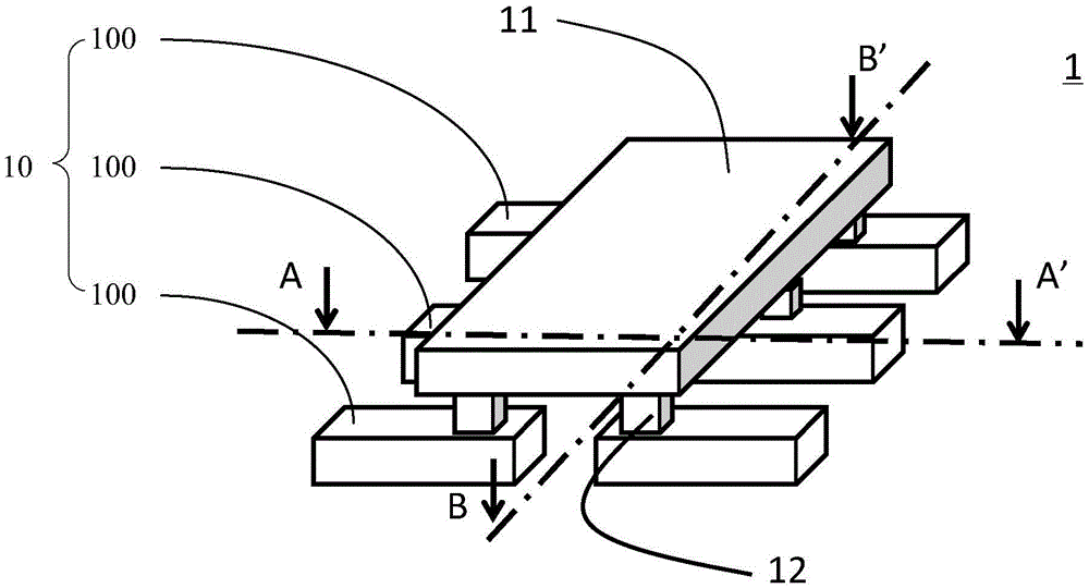
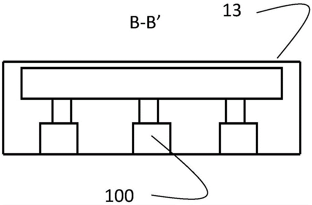
[0052] Please refer to Figure 4 ~ Figure 6 ,in, Figure 4 It is a three-dimensional schematic diagram of the packaging structure of Embodiment 1 of the present invention; Figure 5 yes Figure 4 AA' sectional view of the package structure shown; Figure 6 yes Figure 4 The BB' cross-section of the package structure shown. Specifically, such as Figure 4~6 As shown, in Embodiment 1 of the present application, the package structure 2 includes: a lead frame 20, a chip layer, an electrical connector 22, and a molding compound 23, the chip layer is located above the lead frame 20, and the chip layer At least one chip 21 is included, and the active surface of the chip 21 is electrically connected to the lead frame 20 through an electrical connector 22; the molding compound 23 encapsulates the chip layer, the electrical connector 22 and the lead frame 20;
[0053] Wherein, the lead frame 20 includes a plurality of pins 200, the side of the pins 200 used to electrically connect...
Embodiment 2
[0069] Please refer to Figure 11 , which is a schematic cross-sectional view of the package structure according to Embodiment 2 of the present invention. Such as Figure 11 As shown, in the second embodiment of the present application, the package structure 3 includes: a lead frame 30, a chip layer, an electrical connector 32, and a molding compound 33, the chip layer is located above the lead frame 30, and the chip layer At least one chip 31 is included, the active surface of the chip 31 is electrically connected to the lead frame 30 through an electrical connector 32; the molding compound 33 encapsulates the chip layer, the electrical connector 32 and the lead frame 30;
[0070] Wherein, the lead frame 30 includes a plurality of pins 300, the side of the pins 300 used to electrically connect the chip 31 is the top surface, and the side opposite to the top surface is the bottom surface, between the top surface and the bottom surface The sides are two opposite first sides a...
Embodiment 3
[0081] Please refer to Figure 13 , which is a schematic cross-sectional view of the packaging structure according to Embodiment 3 of the present invention. Such as Figure 13 As shown, in the third embodiment of the present application, the packaging structure 4 includes: a lead frame 40, a chip layer, an electrical connector 42, and a molding compound 43, the chip layer is located above the lead frame 40, and the chip layer At least one chip 41 is included, and the active surface of the chip 41 is electrically connected to the lead frame 40 through an electrical connector 42; the molding compound 43 encapsulates the chip layer, the electrical connector 42 and the lead frame 40;
[0082] Wherein, the lead frame 40 includes a plurality of pins 400, the side of the pins 400 used to electrically connect the chip 41 is the top surface, and the side opposite to the top surface is the bottom surface, between the top surface and the bottom surface The sides are two opposite first ...
PUM
 Abstract
Description
Claims
Application Information
 - R&D
- Intellectual Property
- Life Sciences
- Materials
- Tech Scout
- Unparalleled Data Quality
- Higher Quality Content
- 60% Fewer Hallucinations
Browse by: Latest US Patents, China's latest patents, Technical Efficacy Thesaurus, Application Domain, Technology Topic, Popular Technical Reports.
© 2025 PatSnap. All rights reserved.Legal|Privacy policy|Modern Slavery Act Transparency Statement|Sitemap|About US| Contact US: help@patsnap.com