Laminated module and interposer used in same

A stacking module and intermediary technology, applied in the field of stacking modules, can solve problems such as thermal instability of stacking modules, achieve the effects of suppressing temperature rise, high cooling capacity, and suppressing heat conduction

Inactive Publication Date: 2014-04-23
ZYCUBE
View PDF5 Cites 0 Cited by
  • Summary
  • Abstract
  • Description
  • Claims
  • Application Information

AI Technical Summary

Problems solved by technology

If there are semiconductor devices sensitive to operating temperature on the upper layer of the stacked module, it may cause thermal instability of the stacked module as a whole

Method used


Image

  • Laminated module and interposer used in same
  • Laminated module and interposer used in same
  • Laminated module and interposer used in same

Examples


Embodiment 1

[0311] (the stacked module of Embodiment 1, and the interposer used)

[0312] Figure 21A ~ Figure 21C It is the interlayer 70 used in Embodiment 1 to increase the cooling effect by utilizing the adiabatic expansion of the fluid. Figure 21A is its exploded stereogram, Figure 21B is its stereogram, Figure 21C is its cross-sectional view.

[0313] In the interposer 70, at least one of the heat radiation layer 61b and the heat reflective layer 61a used by the interposer 30 can be used,

[0314] Interposer 70 as Figure 21A ~ Figure 21C As shown, it consists of a rectangular plate-shaped upper wall 73, a rectangular plate-shaped lower wall 74, a pair of side walls 72a and 72b, and the four members form a channel 71 inside. The side walls 72a and 72b are symmetrical in shape, and the channel 71 becomes wider in a certain range from the upstream end and narrows in a certain range from the downstream end. Between the wide part and the narrow part on the upstream side of the ...

Embodiment 2

[0322] (Example 2 stacked module package structure and interposer used)

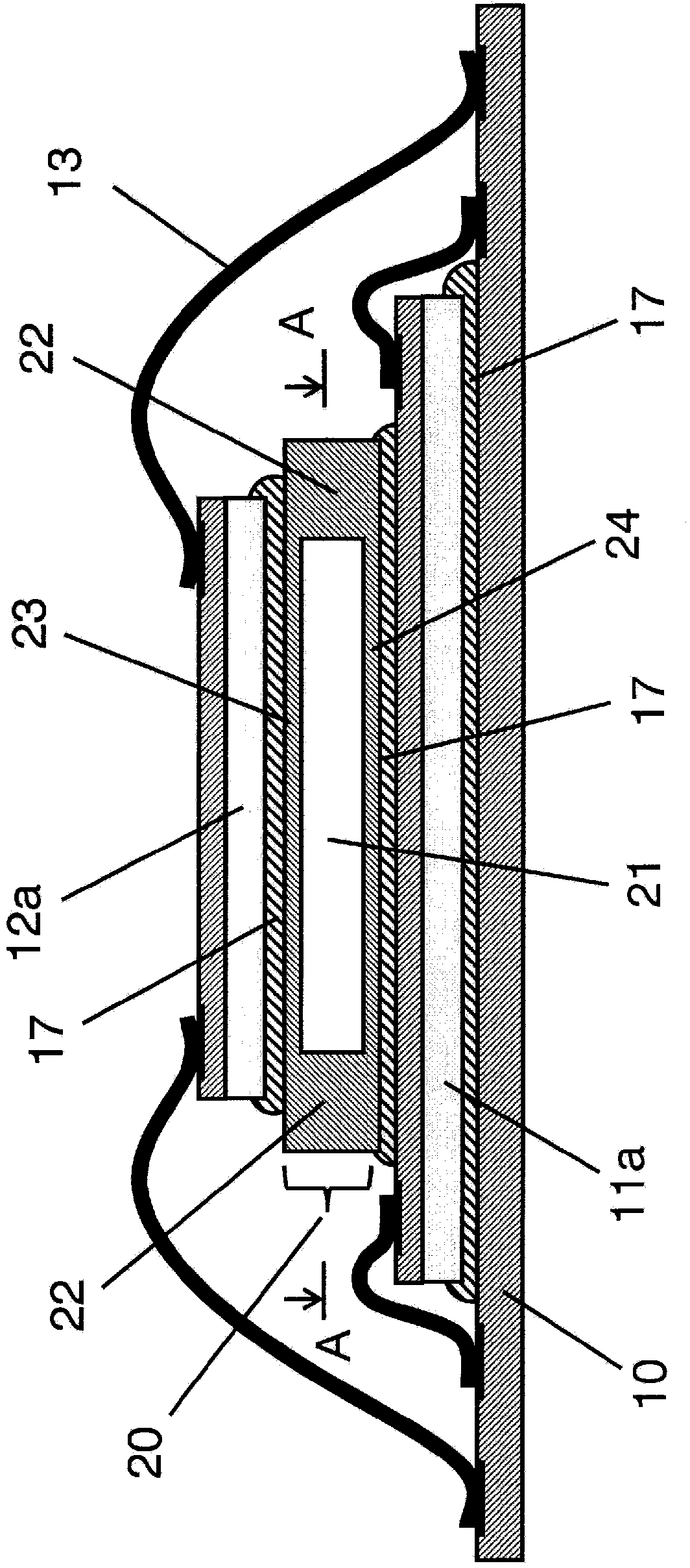
[0323] Figure 23A yes Figure 21A ~ Figure 21C Interposer 70 shown assembled in Figure 3A and Figure 3B The package structure of the stacked module in Embodiment 2 formed by penetrating the electrode module is shown. Figure 23B Channels 71 of interposer 70 are shown.

[0324] Figure 23A The packaging structure, except for the interposer 70 that replaces the interposer 30, the rest are the same as Figure 3A and Figure 3B The bonding modules shown are the same, and descriptions are omitted here. Figure 23A In , the fluid L flows from the front of the paper to the rear along the direction perpendicular to the paper.

[0325] Figure 23A The same is true for the package structure, and an interposer 70 having an "adiabatic expansion structure" is arranged between the first semiconductor device 11b on the lower side and the second semiconductor device 12b on the upper side, and Figure 22A Si...


PUM


Abstract

Provided is a laminated module that can suppress a temperature rise accompanying the heat release of semiconductor devices, allowing stable operation, even in the case of a configuration laminating semiconductor devices having large power consumption. The laminated module is provided with: an interposer (70) having a channel (71) through which a fluid flows; at least one first semiconductor device disposed on one side of the interposer (70); and at least one second semiconductor device disposed at the reverse surface of the interposer (70) from the first semiconductor device. The channel (71) of the interposer (70) has a first region having a cross-sectional area that is relatively smaller and a second region having a cross-sectional area that is relatively larger, and is configured in a manner so that the fluid is subjected to adiabatic expansion partway along moving from the first region to the second region.

Description

technical field [0001] The present invention is a stacking module (hereinafter also referred to as a stacking device module) formed by stacking a plurality of semiconductor devices. Furthermore, it is a stacking module that can suppress the temperature rise of high-power semiconductor devices to ensure stable operation and the used Interposer. Background technique [0002] In recent years, the semiconductor industry represented by silicon has made great technological progress. Regardless of industry and people's livelihood, the miniaturization, light weight, low price, and high functionality of equipment or systems all benefit from this. On the other hand, expectations for higher integration, higher speed, and higher functionality of semiconductor devices have not stopped, including miniaturization. [0003] As a countermeasure, the size of the basic unit of the device (such as a transistor) is reduced to achieve the purpose of increasing the number of devices. The advant...

Claims


Application Information

Patent Timeline
Patent Type & Authority Applications(China)
IPC IPC(8): H01L23/467H01L23/12H01L25/065H01L25/07H01L25/18
CPCH01L2225/06572H01L2224/16145H01L2224/73204H01L25/0657H01L23/49827H01L2224/48227H01L2225/06517H01L2225/06575H01L2225/06589H01L2224/32145H01L2924/15311H01L2225/0651H01L23/473H01L2224/48472H01L2224/16225H01L2224/48091H01L24/75H01L2224/73265H01L2224/32225H01L24/73H01L2924/00H01L2924/00012H01L2924/00014
Inventor 中村博文盆子原学
Owner ZYCUBE
Why Eureka
Try Eureka