Photoelectric conversion circuit used for visible light sensor

A photoelectric conversion circuit and visible light technology, which is applied in the measurement circuit and the use of electrical radiation detectors for light metering, etc. The effect of visible light component noise

Active Publication Date: 2014-04-30
XIDIAN UNIV
View PDF12 Cites 10 Cited by
  • Summary
  • Abstract
  • Description
  • Claims
  • Application Information

AI Technical Summary

Problems solved by technology

[0004] However, since the light source of the visible light sensor is generally natural light, light, etc., which have a wide spectrum, the photodiode will respond to other spectra outside the visible light band, such as infrared light, so that figure 1 The current generated by the photodiode in the structure shown includes not only the current converted from visible light, but also the current converted from non-visible light. These currents are input into the analog-to-digital conversion circuit, which will cause the visible light sensor to fail to sense the intensity of visible light. precise
At the same time, since the photodiode itself will generate a dark current that varies with temperature and has nothing to do with the illuminance, the photocurrent generated by the photodiode is not completely proportional to the illuminance. figure 1 In the structure shown, the dark current generated by the photodiode is directly input to the analog-to-digital conversion circuit without processing, which will also lead to inaccurate sensing of the visible light intensity by the visible light sensor.

Method used


Image

  • Photoelectric conversion circuit used for visible light sensor
  • Photoelectric conversion circuit used for visible light sensor
  • Photoelectric conversion circuit used for visible light sensor

Examples


Embodiment Construction

[0022] The present invention will be further described below in conjunction with accompanying drawings and embodiments thereof.

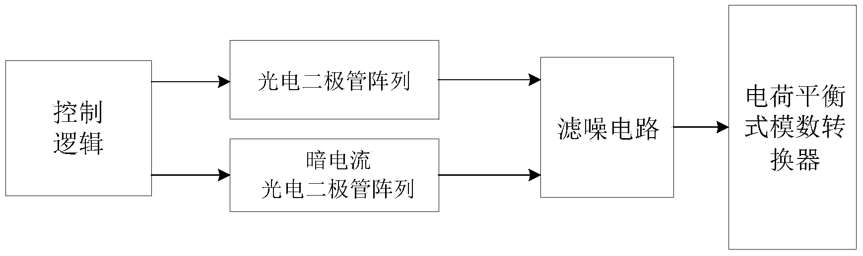
[0023] refer to figure 2 , the photoelectric conversion circuit of the present invention includes a photodiode array 1, a dark current diode array 2 and a noise filter circuit 3;

[0024] The photodiode array 1 includes 64 photodiodes, and optical coatings are arranged on the top of these photodiodes, and the optical response thereof is similar to that of an illuminance meter. The 64 photodiodes are connected in parallel, the actual number of access circuits is selected by control logic, the positive pole is connected to the ground potential, and the negative pole is connected to the first input end of the noise filter circuit 3; Photocurrent I 1 Give the noise filter circuit 3.

[0025] The dark current photodiode array 2 includes 64 photodiodes connected in parallel, and metal shielding layers are arranged above these photodiodes, which do not...


PUM


Abstract

The invention discloses a photoelectric conversion circuit used for a visible light sensor chip. The photoelectric conversion circuit mainly solves the problem that in the prior art, visible light sensing accuracy is influenced by dark current noise. The photoelectric conversion circuit comprises a photoelectric diode array (1), a dark current photoelectric diode array (2) and a noise filtering circuit (3). The number of diodes, connected into the circuit actually, of the photoelectric diode array and the number of diodes, connected into the circuit actually, of the dark current photoelectric diode array are controlled through external control logic. The first input end of the noise filtering circuit is connected with the output end of the photoelectric diode array, the second input end of the noise filtering circuit is connected with the output end of the dark current photoelectric diode array, subtraction is performed on light currents generated by the photoelectric diode array and containing dark currents and dark currents generated by the dark current photoelectric diode array through the noise filtering circuit so as to obtain visible light currents without the dark currents, and the visible light currents are output to an external charge balance type analog-to-digital conversion circuit. The photoelectric conversion circuit improves the photoelectric conversion accuracy, restrains influences on visible light sensing results of the dark current noise, and improves the visible light sensing accuracy.

Description

technical field [0001] The invention belongs to the technical field of electronic circuits, relates to a photoelectric conversion circuit and can be used in visible light sensors. Background technique [0002] Many electronic devices such as smartphones, game consoles, computers, and TVs use visible light sensors to quantify the light output and then adjust the backlight through control logic to improve the user's visual experience, extend battery life, and improve power efficiency. As one of the most important components of the visible light sensor, the photoelectric conversion circuit's conversion accuracy greatly restricts the accuracy of the entire visible light sensor system. [0003] figure 1 Shown is a conventional photoelectric conversion system block diagram for visible light sensors. It includes control logic circuit, photodiode, analog-to-digital conversion circuit. During the detection of visible light, the photodiode is connected to the circuit through the co...

Claims


Application Information

Patent Timeline
Patent Type & Authority Applications(China)
IPC IPC(8): G01J1/44
Inventor 何惠森来新泉陈新邵丽丽
Owner XIDIAN UNIV
Why Eureka
Try Eureka