A two-dimensional material composite multicolor infrared detection chip with a hollow surface plasmon structure

A technology of surface plasmons and two-dimensional materials, applied in electrical components, radiation control devices, semiconductor devices, etc., can solve the problems of narrow response spectrum range, low responsivity, and low detection rate, and achieve infrared spectrum enhancement Effects of response, enhanced absorption, and suppression of dark current noise

Active Publication Date: 2021-11-05
SOUTHEAST UNIV
View PDF4 Cites 0 Cited by
  • Summary
  • Abstract
  • Description
  • Claims
  • Application Information

AI Technical Summary

Problems solved by technology

[0005] The purpose of the present invention is to solve the bottleneck problems such as narrow response spectrum range, low resolution, low detection rate and low responsivity of existing infrared detectors.

Method used


Image

  • A two-dimensional material composite multicolor infrared detection chip with a hollow surface plasmon structure
  • A two-dimensional material composite multicolor infrared detection chip with a hollow surface plasmon structure
  • A two-dimensional material composite multicolor infrared detection chip with a hollow surface plasmon structure

Examples


Embodiment 1

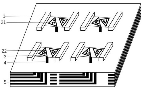
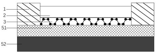
[0028] Embodiment 1: see Figure 1-Figure 4 , a two-dimensional material composite multicolor infrared detection chip with a hollow surface plasmon structure, a single chip includes a plurality of detectors, and the detectors are electrode 1, surface plasmon layer 2, A two-dimensional material layer 3 , an electrical channel 4 , and a CMOS circuit 5 . Among them, the two-dimensional material layer 3 is designed in an array shape by PDMS technology, and then undergoes epitaxial growth. The two-dimensional material can also be grown by chemical vapor deposition, and then the array structure can be carved out by photolithography. The plasmonic layer includes a hollow metal plate and metal nanoparticles, wherein the hollow metal plate is deposited on the two-dimensional material layer, and the metal nanoparticles are deposited in or outside the hollow area of ​​the metal plate. The plasmonic layer can localize the incident light in the tip area of ​​the hollow triangular plate a...


PUM

PropertyMeasurementUnit
sizeaaaaaaaaaa
sizeaaaaaaaaaa
thicknessaaaaaaaaaa

Abstract

The present invention designs a two-dimensional material composite multicolor infrared detection chip with a hollow surface plasmon structure. The parts of a single chip are metal electrodes (1) and surface plasmon layers (2) from top to bottom. ), a two-dimensional material layer (3), an electrical channel (4), and a CMOS readout circuit (5), the two-dimensional material mid-infrared detector of the present invention can complete the response to visible light and infrared light. Compared with some existing infrared detectors, it has the advantages of visible / infrared multicolor detection, mid-infrared band spectral response, high responsivity, high detection rate, and high resolution.

Description

technical field [0001] The invention belongs to the field of light detection technology and metal nanomaterials, in particular to a hollow surface plasmon structure / two-dimensional material composite multicolor infrared detection chip array device. Background technique [0002] Infrared detection chip occupies a core position in the infrared field. It can provide stable observation in harsh weather conditions or dark environments. It is widely used in aerospace, infrared guidance, security alarms, automatic driving, environmental monitoring, and weather satellites. It is a relationship It is an important device for the development of cutting-edge technology industry and the national economy and people's livelihood. With the continuous expansion of the demand for infrared detection, the above-mentioned fields have higher and higher requirements for the detection performance and detection methods of infrared detection chips. Direction of development. However, the shortcoming...

Claims


Application Information

Patent Timeline
Patent Type & Authority Patents(China)
IPC IPC(8): H01L27/144H01L31/0216
CPCH01L27/1443H01L27/1446H01L31/02161
Inventor 张彤吴静远何伟迪苏丹张晓阳
Owner SOUTHEAST UNIV
Why Eureka
Try Eureka