Power supply installation structure of light-emitting diode (LED) lamp
A technology of LED lighting and installation structure, which is applied in the direction of lighting devices, parts of lighting devices, lighting and heating equipment, etc. It can solve the problems that affect the shape design of lamps, the PCB board takes up a lot of space, and the processing procedures are cumbersome. The effect of large-scale promotion and application, simplified installation process and reduced production cost
- Summary
- Abstract
- Description
- Claims
- Application Information
AI Technical Summary
Problems solved by technology
Method used
Image
Examples
Embodiment 1
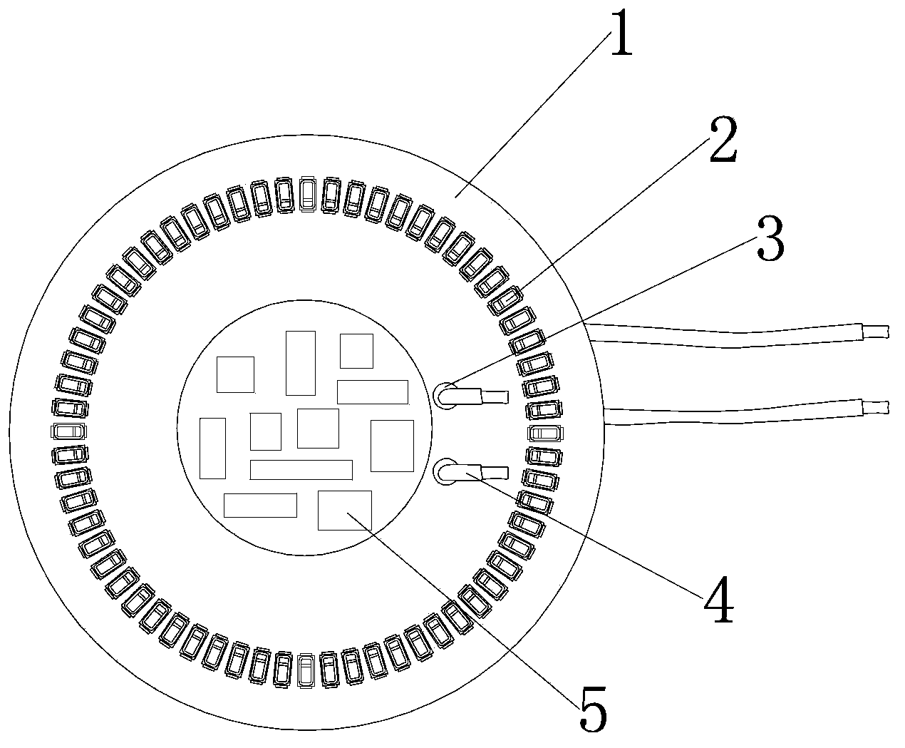
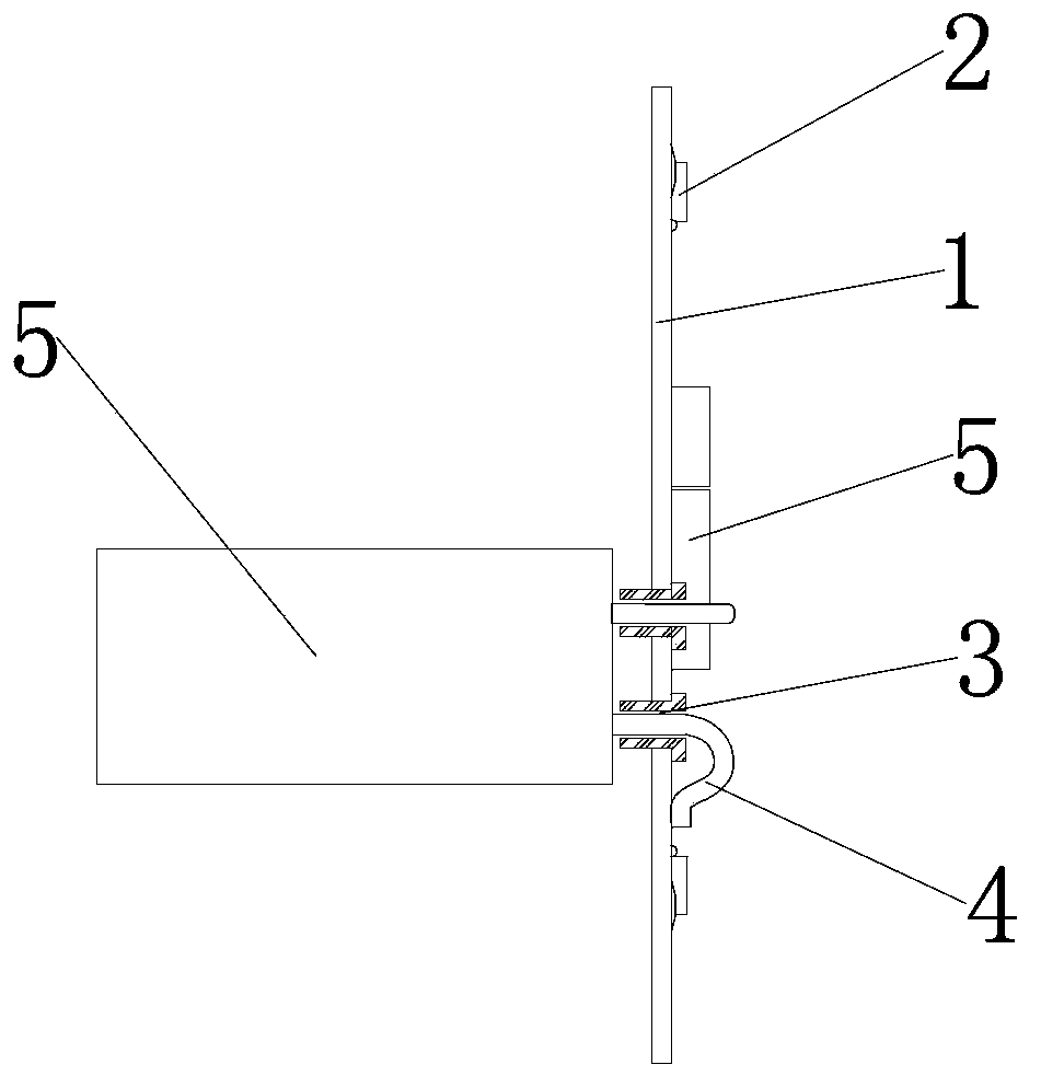
[0022] Embodiment one: with reference to attached Figure 1-2 This embodiment includes a heat dissipation substrate 1, LED2, electronic components 5 and wires 4, the wires 4 are connected to the electronic components 5, the electronic components 5 are welded in the middle of the upper surface of the heat dissipation substrate 1, and the heat dissipation substrate 1 is provided with a round hole 3, Wire 4 is welded on the upper surface of heat dissipation substrate 1 through circular hole 3 from below heat dissipation substrate 1 , heat dissipation substrate 1 is arranged in a circular shape, and LEDs 2 are arranged in a ring and welded on the edge of heat dissipation substrate 1 upper surface.
[0023] The assembly process of this embodiment: first arrange the LEDs 2 in a ring and weld them on the edge of the upper surface of the heat dissipation substrate 1, and then fix the electronic components 5 in the middle of the heat dissipation substrate 1 by tin or tin-lead welding. ...
Embodiment 2
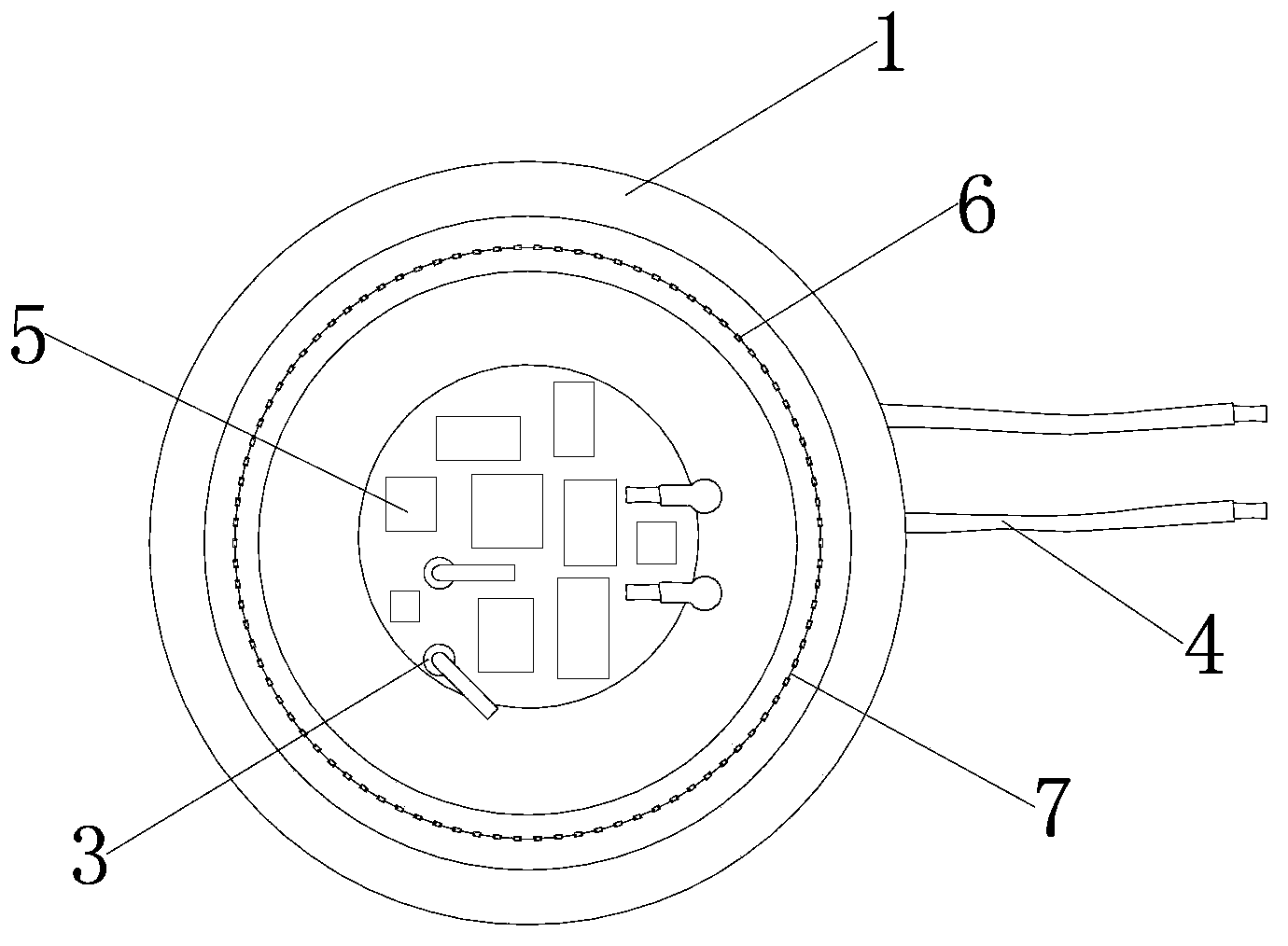
[0024] Embodiment two: with reference to attached Figure 3-5 This embodiment includes heat dissipation substrate 1, electronic components 5 and wires 4, LED package 2 includes LED chips 6, gold wires 7, cured glue 8 mixed with phosphor powder, wires 4 are connected to electronic components 5, LED chips 6, The gold wire 7 is set inside the cured glue 8, the LED chip 6 is glued on the upper surface of the heat dissipation substrate 1 and connected to the heat dissipation substrate 1 through the gold wire 7, and the electronic component 5 is welded in the middle of the upper surface of the heat dissipation substrate 1, and the heat dissipation substrate 1 A round hole 3 is provided, and the wire 4 passes through the round hole 3 from the bottom of the heat dissipation substrate 1 and is welded on the upper surface of the heat dissipation substrate 1 . at the edge.
[0025] The assembly process of this embodiment: first arrange the LED chips 6 in a ring shape and glue them on th...
PUM
 Abstract
Description
Claims
Application Information


