Integration method for increasing luminous power of LED

An integrated method and power technology, applied in the direction of electrical components, circuits, semiconductor devices, etc., can solve the problems of increasing the chip area of ​​light-emitting diodes, reducing the number of devices, and contradicting the low cost of light-emitting diodes, so as to achieve high-power light output , Increased luminous power, solve the effect of low quantum efficiency

Inactive Publication Date: 2014-05-07
甘志银
View PDF8 Cites 6 Cited by
  • Summary
  • Abstract
  • Description
  • Claims
  • Application Information

AI Technical Summary

Problems solved by technology

However, both of the above two solutions need to increase the chip area of ​​the light-emitting diode, so that the number of devices on a single wafer is greatly reduced
This is contrary to the development of light-emitting diodes in the direction of low cost

Method used


Image

  • Integration method for increasing luminous power of LED
  • Integration method for increasing luminous power of LED
  • Integration method for increasing luminous power of LED

Examples


Embodiment 1

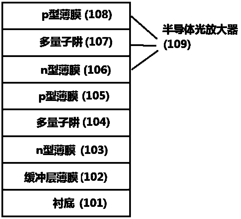
[0015] Growth of LED epitaxial thin films on metal-organic chemical vapor deposition, molecular beam epitaxy, and hydride vapor phase epitaxy equipment, see figure 1 On the substrate 101, the epitaxial buffer layer film system 102, n-type film system 103, multi-quantum well system 104, and p-type film system 105 are sequentially formed from bottom to top to form the basic LED epitaxial structure, and continue on the basic LED epitaxial structure The epitaxial n-type thin film system 106 , the multi-quantum well system 107 and the p-type thin film system 108 form a semiconductor optical amplifier 109 . The various films in the LED epitaxial film are single-layer films or multi-layer doped films or heterojunction film layers.

[0016] The film systems between the cascades, such as the p-type thin film system 105 and the n-type thin film system 106, can adopt the same gradient doping or heterojunction doping structure in order to reduce the voltage drop, improve the effective inj...

Embodiment 2

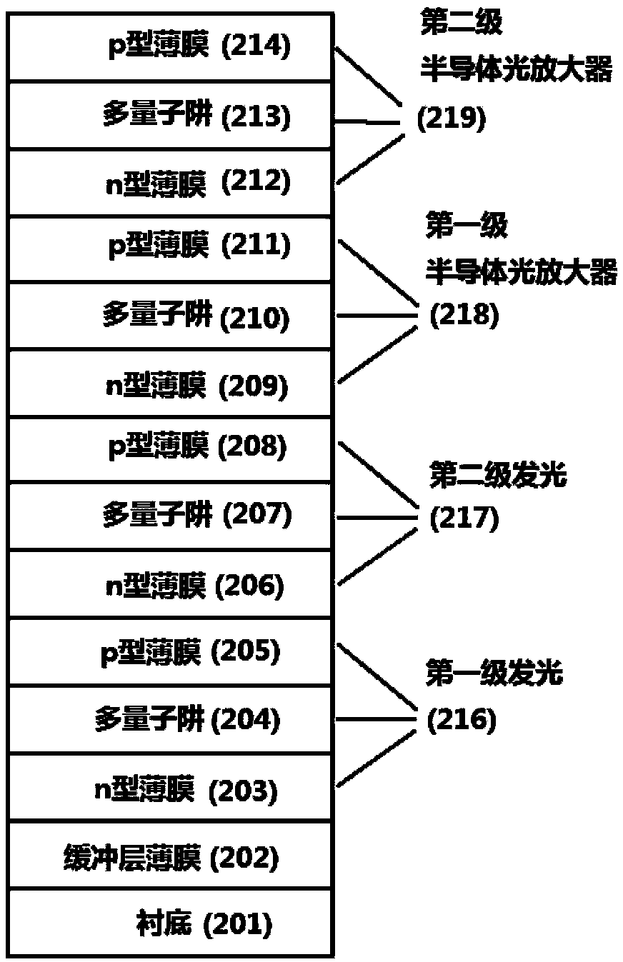
[0019] Extend the LED epitaxial film to a multi-level LED series structure. In the traditional LED chip structure, multi-section LED structures are added along the epitaxial growth direction, such as figure 2 As shown on the substrate 201, from bottom to top, epitaxial buffer layer film system 202, n-type film system 203, multi-quantum well system 204, p-type film system 205, n-type film system 206, multi-quantum well system 207, p-type film system Thin-film system 208, n-type thin-film system 209, multiple quantum well system 210, p-type thin-film system 211, n-type thin-film system 212, multiple quantum well system 213, p-type thin-film system 214, wherein n-type thin-film system 203, multiple quantum well system 204 and p-type thin film system 205 form the first-level light-emitting unit 216, and the n-type thin-film system 206 above the first-level light-emitting unit 216, the multi-quantum well system 207 and the p-type thin-film system 208 form the second-level light-em...

Embodiment 3

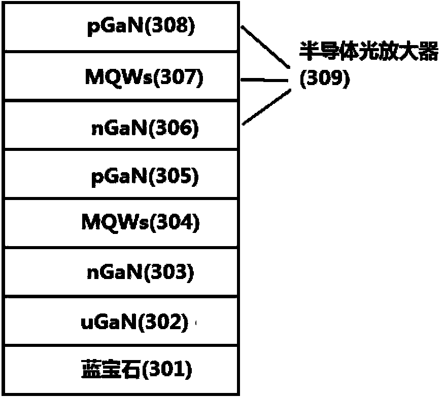
[0022] Embodiment three is the same as embodiment one, the difference is as follows image 3 As shown, the blue GaN-based LED epitaxial film is grown on the sapphire substrate of this embodiment, and uGaN302, nGaN303, InGaN-based MQWs304, pGaN305, nGaN306, InGaN-based MQWs307, and pGaN308 are epitaxially grown on the sapphire 301 from bottom to top. Among them, nGaN306, MQWs307 and pGaN308 form a semiconductor optical amplifier. The basic principle of increasing the luminous power of the LED is that the light emitted by the InGaN-based MQWs304 passes through the semiconductor optical amplifier and is amplified by stimulated radiation, thereby increasing the luminous power of the LED.


PUM


Abstract

Disclosed is an integration method for increasing luminous power of an LED. The method comprises successively growing a buffer layer film system, an n-type film system, a multi-quantum well system and a p-type film system from the bottom to the top on a substrate in an epitaxial mode to form a conventional LED epitaxial structure, and continuing growing an additional n-type film system, an additional multi-quantum well system and an additional p-type film system on the LED epitaxial structure in an epitaxial mode to form a semiconductor amplifier. Provided by the invention is also a multi-section LED structure additionally arranged in a conventional LED chip structure along an epitaxial growth direction. The advantages are as follows: a structure provided with light amplification gains is added in the growth direction of a conventional LED chip structure so that the light extraction efficiency is substantially increased, at the same time, the luminescence area of a chip is not enlarged, and the device actual production power of a single wafer is effectively improved; and the multi-section LED structure is additionally arranged in the conventional LED chip structure along an epitaxial growth direction so that an LED chip has the effect of multi-stage series connection, the luminous power is substantially improved, large-power light output is realized, and the chip cost is lowered at the same time.

Description

technical field [0001] The invention belongs to the technical field of semiconductor optoelectronics and relates to a light emitting diode, in particular to a device structure of a high efficiency and high brightness light emitting diode and a manufacturing method thereof. Background technique [0002] A light emitting diode (LED) is a solid-state semiconductor device that converts electrical energy into light. Compared with traditional light sources, such as incandescent lamps and energy-saving lamps, light-emitting diodes have many advantages such as long life, high luminous efficiency, good color rendering, high stability, no radiation, low power consumption, shock resistance, and no pollution. It is the most promising green lighting source in the 21st century. [0003] With the development of lighting market demand, light-emitting diodes must develop in the direction of low cost and high brightness. For the direction of increasing the luminous brightness, there are cur...

Claims


Application Information

Patent Timeline
Patent Type & Authority Applications(China)
IPC IPC(8): H01L33/00
CPCH01L33/08H01L33/0062
Inventor 甘志银严晗
Owner 甘志银
Why Eureka
Try Eureka