
Capacitor and power integrated circuit

A capacitor and electrical connection technology, applied in the field of power device structure design, can solve the problems of large power integrated circuits and high production costs, and achieve an effect that is conducive to popularization and application

Active Publication Date: 2014-05-14
SHENZHEN SUNMOON MICROELECTRONICS
View PDF4 Cites 0 Cited by
  • Summary
  • Abstract
  • Description
  • Claims
  • Application Information

AI Technical Summary

Problems solved by technology

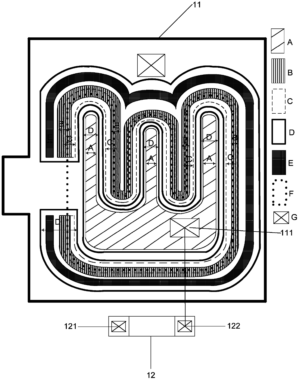
[0004] The purpose of the embodiment of the present invention is to provide a capacitor, aiming to solve the problem of large volume and high production cost of the power integrated circuit in the existing power integrated circuit, because the capacitor is externally connected to the NLDMOS tube.

Method used


Image

  • Capacitor and power integrated circuit
  • Capacitor and power integrated circuit
  • Capacitor and power integrated circuit

Examples


Embodiment 1

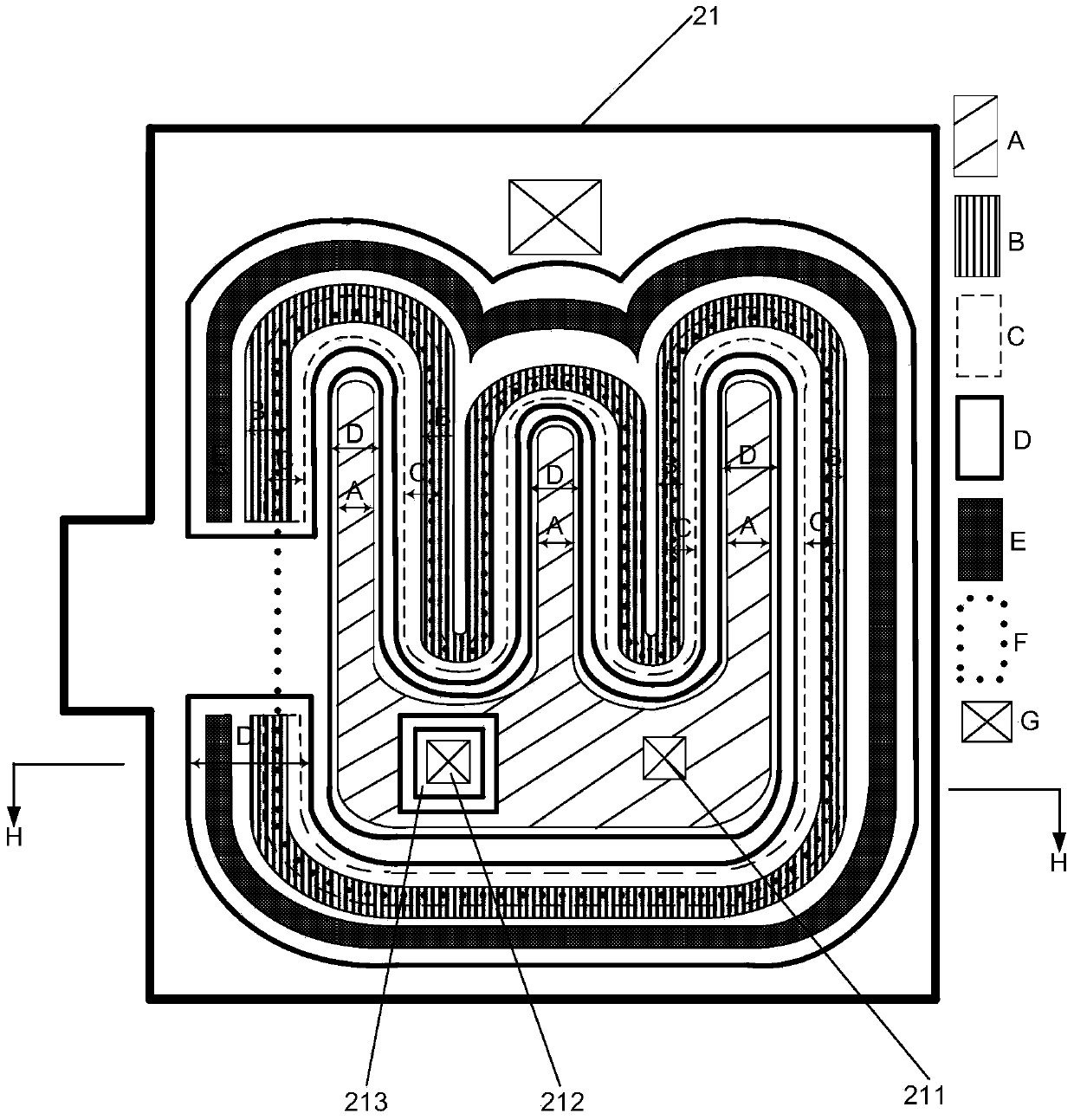
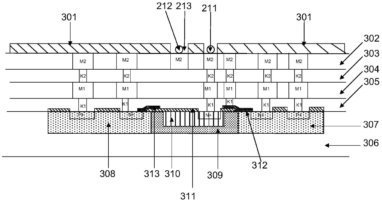
[0014] Embodiment 1 of the present invention provides a field effect transistor, the field effect transistor is an NLDMOS transistor, such as figure 2 as shown, image 3 yes figure 2 The H-H sectional view of the figure shows only the parts related to Embodiment 1 of the present invention for the convenience of description.

[0015] Among them, graph A represents the low-voltage N well region of NLDMOS transistor 21, graph B represents the N+ doped region of NLDMOS transistor 21, graph C represents the POLY polycrystalline layer of NLDMOS transistor 21, graph D represents the top layer metal M2, and graph E represents the NLDMOS transistor The P+ doped region of 21 , the graph F represents the high voltage N well region of the NLDMOS transistor 21 , and the graph G represents the pin PAD of the NLDMOS transistor 21 . combine figure 2 with image 3 As shown, in Embodiment 1 of the present invention, the NLDMOS transistor 21 includes a passivation layer 301 and a P substr...

Embodiment 2

[0019] Embodiment 2 of the present invention provides a power integrated circuit, including a field effect transistor and a capacitor as described in Embodiment 1 above. The field effect transistor may be the NLDMOS transistor 21 described in Embodiment 1, which will not be repeated here.

[0020] In summary, in the capacitor proposed by the present invention, its lower plate is electrically connected to the drain of the field effect transistor, and the lower plate is a part of the well region that includes the drain, and its upper plate is a portion that includes the drain of the field effect transistor. Part of the well region corresponds to the top layer metal, so that the capacitor is integrated into the field effect transistor without increasing the volume of the field effect transistor. If the field effect transistor integrated with the capacitor is applied to a power integrated circuit, the current integrated capacitor can be reduced. The size of the power integrated ci...


PUM


Abstract

The invention, which belongs to the field of the power device structure design, provides a capacitor and a power integrated circuit. A lower polar plate of the capacitor and a drain electrode of a field effect transistor share an active region and the lower polar plate of the capacitor and the drain electrode of the field effect transistor are electrically connected. The lower polar plate of the capacitor is a partial well region containing the drain electrode and an upper polar plate of the capacitor is a top metal corresponding to the partial well region containing the drain electrode of the field effect transistor. More particularly, the drain electrode of the field effect transistor employs an E-shaped layout mode; and the top metal as the upper polar plate is distributed at the sealing port end of the E-shaped layout of the drain electrode of the field effect transistor, so that the capacitor is integrated to the field effect transistor without increasing the size of the field effect transistor. If the field effect transistor integrated with the capacitor is applied to the power integrated circuit, the size of the existing power integrated circuit integrated with the capacitor can be reduced and the production cost can be lowered, so that the product popularization and application can be realized beneficially.

Description

technical field [0001] The invention belongs to the field of power device structure design, in particular to a capacitor and a power integrated circuit. Background technique [0002] In the field of drive circuit design, in order to reduce cost and size, power integrated circuits are often used to realize constant current / constant voltage drive control of loads. A power integrated circuit refers to a special integrated circuit that integrates power devices, low-voltage control circuits, signal processing, and communication interfaces into the same chip. The power device is the core part and occupies most of the chip area. In the constant current / constant voltage drive circuit provided by the prior art, the power integrated circuit uses an N-type lateral double diffused MOS (N Type Lateral Double Diffused MOS, NLDMOS) tube as the power device, and a capacitor C0 is set inside the power integrated circuit , one end of the capacitor C0 is connected to the drain pin of the NLDM...

Claims


Application Information

Patent Timeline
Patent Type & Authority Applications(China)
IPC IPC(8): H01L27/06H01L29/40
Inventor 李照华赵春波林道明戴文芳陈艳霞
Owner SHENZHEN SUNMOON MICROELECTRONICS
Learn More