Manufacturing method of stress sensor based on nanorod diode piezoelectric effect

A technology of stress sensor and piezoelectric effect, applied in the field of preparation of stress sensor, can solve the problems of narrowing of effective bandwidth and red shift of emission wavelength, etc.

Inactive Publication Date: 2014-05-14
INST OF SEMICONDUCTORS - CHINESE ACAD OF SCI
View PDF5 Cites 12 Cited by
  • Summary
  • Abstract
  • Description
  • Claims
  • Application Information

AI Technical Summary

Problems solved by technology

[0002] In the heteroepitaxy nanopillar semiconductor diode array, because of the piezoelectric effect, there is a large piezoele

Method used


Image

  • Manufacturing method of stress sensor based on nanorod diode piezoelectric effect
  • Manufacturing method of stress sensor based on nanorod diode piezoelectric effect
  • Manufacturing method of stress sensor based on nanorod diode piezoelectric effect

Examples


Embodiment Construction

[0019] In order to make the object, technical solution and advantages of the present invention clearer, the present invention will be further described in detail below in conjunction with specific embodiments and with reference to the accompanying drawings.

[0020] see Figure 1 to Figure 7 , the present invention provides a method for preparing a stress sensor based on the nanocolumn diode piezoelectric effect, comprising the following steps:

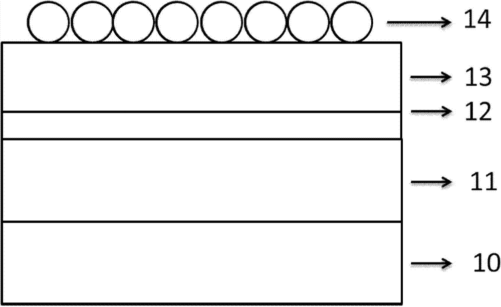
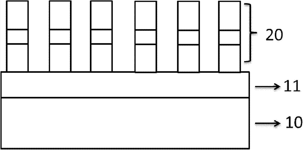
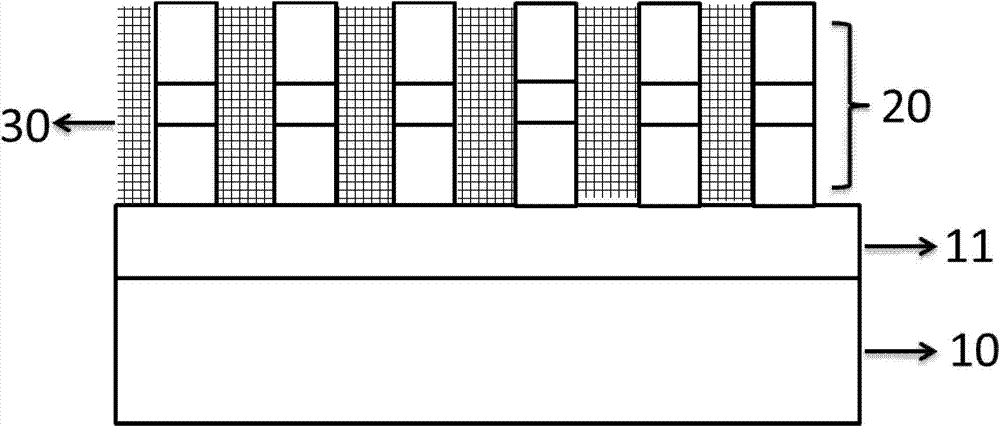
[0021] Step 1: Take a substrate 10, grow a layer of thin film n-type GaN11 on the substrate 10, then grow a layer of multi-quantum well active region, that is, MQWs12 and p-type GaN, that is, p-GaN13; finally, p-GaN13 , forming a complete LED structure, and finally self-assemble a layer of densely arranged nanosphere array 14 on the surface of p-GaN13; wherein, the substrate 10 is a sapphire substrate, and can also be glass, Si, ZnO, AlN, SiC , GaN, GaAs, LiAlO 2 Other III / V, IV / VI binary, ternary and quaternary compound semiconduct...


PUM

PropertyMeasurementUnit
Thicknessaaaaaaaaaa

Abstract

The invention discloses a manufacturing method of a stress sensor based on the nanorod diode piezoelectric effect. The method comprises the steps that an n-type layer, a multi-quantum-well active area and a p-type layer sequentially grow on a substrate, and a nanometer small ball array is assembled on the upper surface of the p-type layer; the nanometer small ball array is adopted as a mask, an LED structure is etched, the etching depth makes contact with the n-type layer, and a nanorod LED array is formed; transparent materials fill the gaps among the nanorod LED array; a metal conductive layer deposits on the surface of the nanorod LED array; part of the n-type layer is exposed through etching, and an n-type electrode and a p-type electrode are manufactured on the upper surface of the exposed n-type layer and the metal conductive layer through a metal evaporation method; a transparent rigid base plate is pressed on the part, not provided with the p-type electrode, of the surface of the metal conductive layer; the n-type electrode and the p-type electrode are communicated, and manufacturing of the stress sensor is finished.

Description

technical field [0001] The invention relates to the technical field of semiconductors, in particular to a method for preparing a stress sensor based on the piezoelectric effect of a nanocolumn diode. Background technique [0002] In the heteroepitaxial nanopillar semiconductor diode array, because of the piezoelectric effect, there is a large piezoelectric field, which will tilt the diode energy band, narrow the effective bandwidth, and red-shift the luminous wavelength. The piezoelectric electric field changes with the external pressure. That is to say, under the change of external pressure, the effective bandwidth of the quantum well in the active region will be made, so that the wavelength and color of the light emitted by the diode will also change with the external pressure, so that the magnitude of the external stress can be observed intuitively, so that Realize the alarm function. For example, it is applied to the weight limit alarm of passing vehicles on the bridge...

Claims


Application Information

Patent Timeline
IPC IPC(8): H01L41/22G01L1/16B82Y15/00
Inventor 魏同波吴奎王军喜曾一平李晋闽
Owner INST OF SEMICONDUCTORS - CHINESE ACAD OF SCI
Why Eureka
Try Eureka