Trench-type MOS rectifier and manufacturing method thereof

A manufacturing method and ditch technology, applied in semiconductor/solid-state device manufacturing, semiconductor devices, electrical components, etc., can solve problems such as high leakage current, reduced reliability, and reduced forward and reverse surge capabilities of Schottky diodes , to achieve the effect of low forward bias voltage and small reverse leakage

Active Publication Date: 2014-05-28
CHIP INTEGRATION TECH +1
View PDF5 Cites 4 Cited by
  • Summary
  • Abstract
  • Description
  • Claims
  • Application Information

AI Technical Summary

Problems solved by technology

However, the leakage current of Schottky diodes is higher than that of ordinary PN diodes, and the leakage current is not a stable value but increases with the increase of reverse bias voltage. This is because the image charge potential barrier lowering
Another major disadvantage is that the reliability of the metal-semiconductor contact decreases as the temperature rises, which reduces the Schottky diode's ability to withstand forward and reverse surges.

Method used


Image

  • Trench-type MOS rectifier and manufacturing method thereof
  • Trench-type MOS rectifier and manufacturing method thereof
  • Trench-type MOS rectifier and manufacturing method thereof

Examples


Embodiment Construction

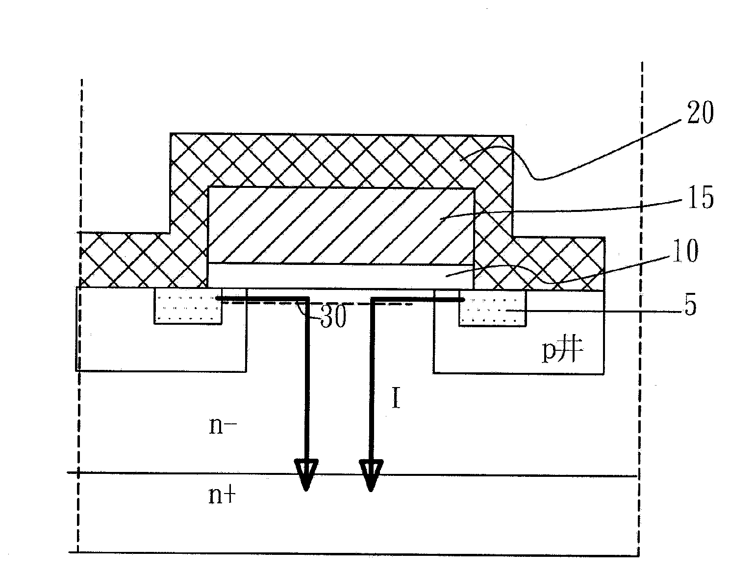
[0046] The present invention discloses a trench-type MOS device structure, comprising: a planar MOS structure is formed on a platform of an active region, and an adjacent side of the platform has a trench in the active region. The active region trench is formed in the n- epitaxial layer on the heavily doped n+ semiconductor substrate. The active region trench has a trench gate oxide layer formed on the bottom and sidewalls of the trench and a p-type doped polysilicon layer formed thereon. A top metal layer is formed on the active region, connecting the gate and source of the planar MOS structure and the polysilicon layer of the active region trench.

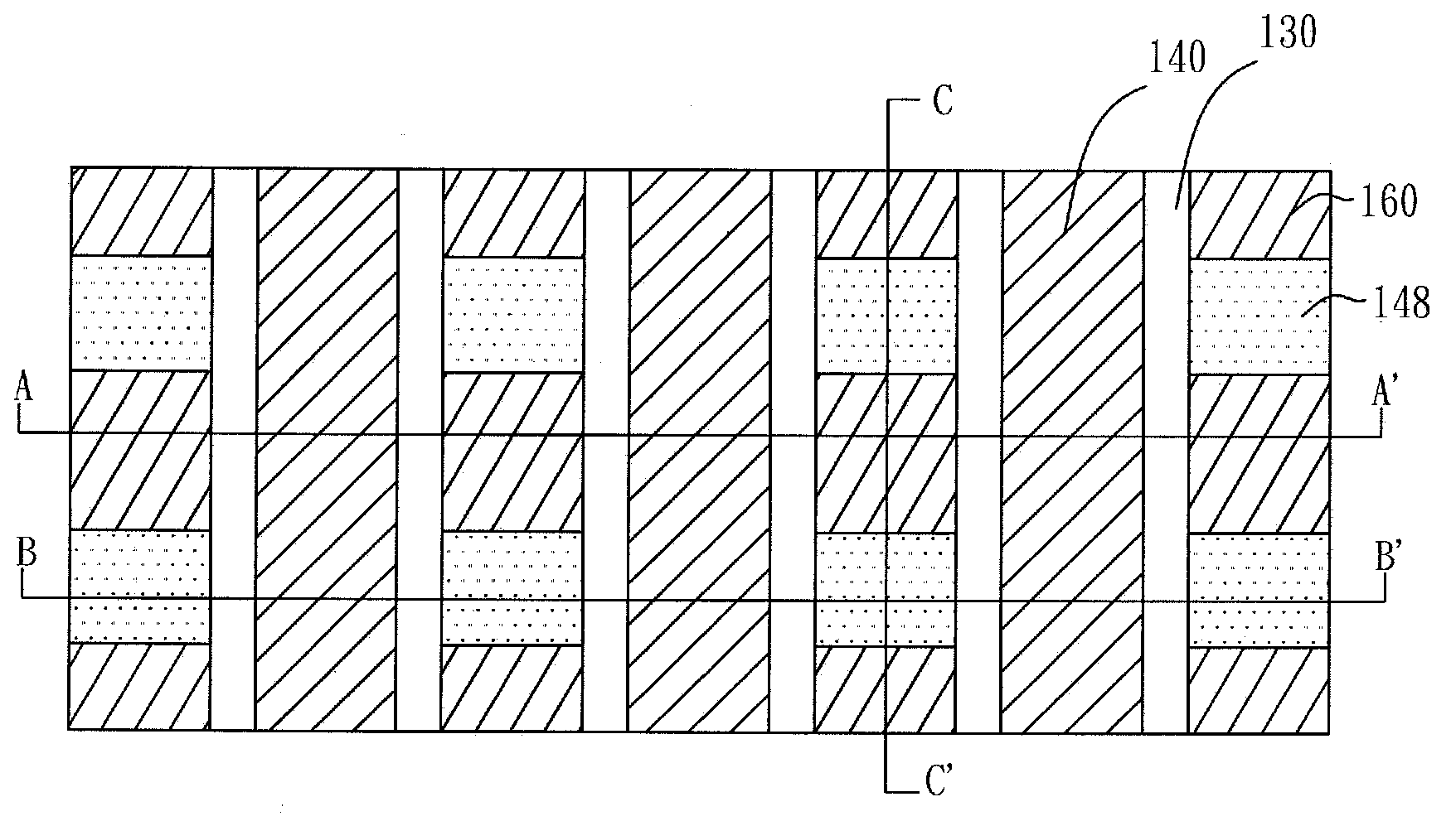
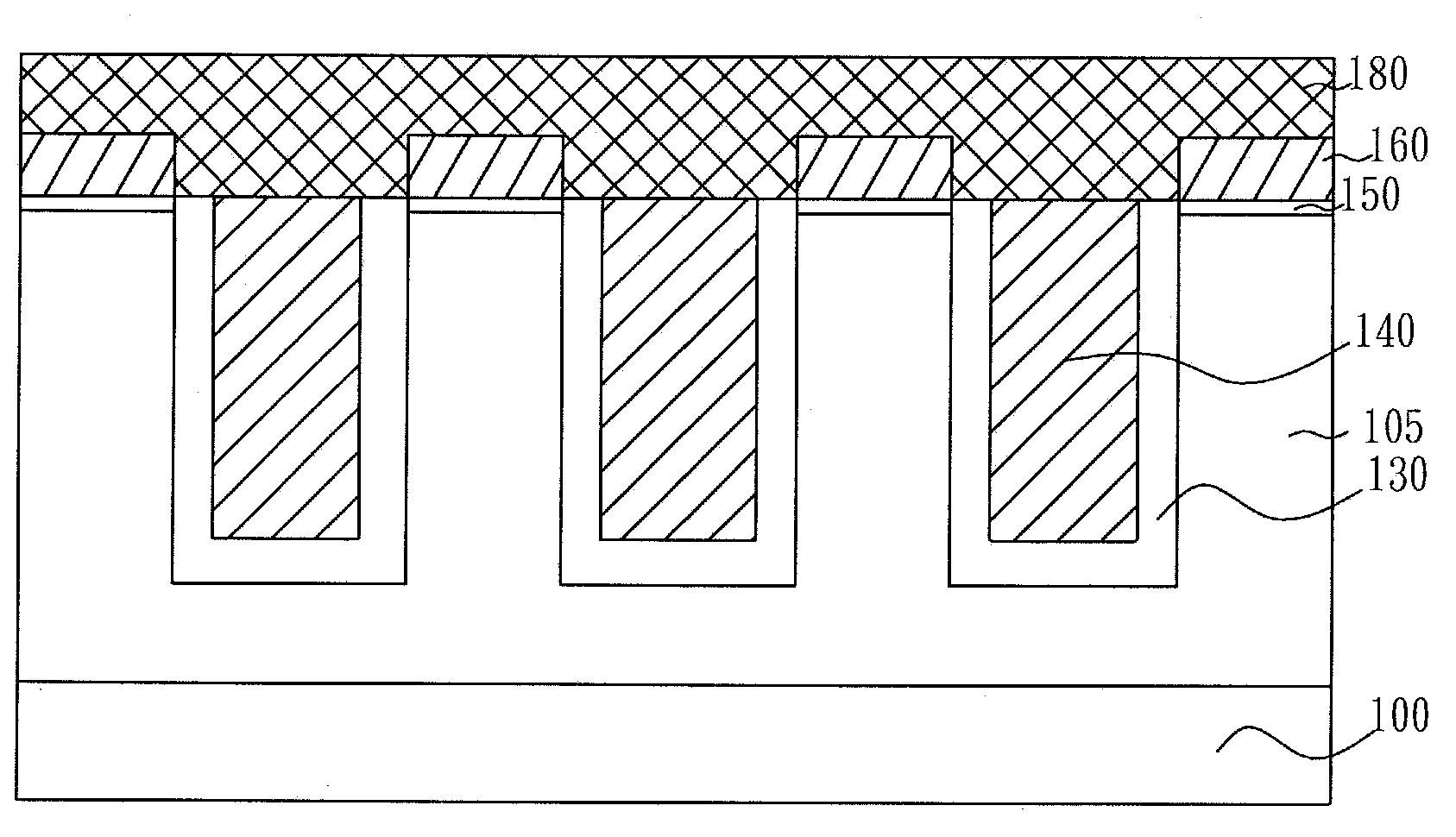
[0047] The structure of the trenched MOS device structure (excluding the top metal layer) of the present invention with multi-platform and multi-active region trenches, please refer to Figure 2A Top view shown. Figure 2B show edge Figure 2A A schematic diagram of the cross-section of the trench MOS device on the A-A' line. ...


PUM


Abstract

The invention discloses a structure of a trench-type MOS rectifying element structure. The structure includes: a planar MOS rectifying structure is formed on platforms of an active zone and adjacent edges of the platforms are provided with active-zone trenches which are formed in an n- epitaxial layer of a heavily doped n+ semiconductor substrate. In the active-zone trenches, trench gate oxide layers are formed at the bottom parts and side walls of the trenches and p-type doped polycrystalline silicon layers are formed on the trench gate oxide layers. A top-part metal layer is formed on the active zone and connected with a grid electrode and a source electrode of the planar MOS structure and the polycrystalline silicon layers of the active-zone trenches. The invention also discloses a manufacturing method of the trench-type MOS rectifying element structure. The trench-type MOS rectifying element structure and the manufacturing method thereof use the trench-type structure so that the forward bias voltage VF is lower and reverse electricity leakage is smaller.

Description

technical field [0001] The present invention relates to semiconductor elements, in particular to a novel trench-type MOS rectifier diode structure and a manufacturing method thereof. Background technique [0002] Schottky diodes are an important power component and are widely used in power supply switches, motor controls, telecom switches, factory automation, electronic automation, etc. and many high-speed power switching applications. The attractiveness of Schottky diodes lies in their good performance, such as reasonable leakage current under reverse bias (Schottky diode leakage current is higher than that of general PN diodes), low forward bias The voltage and reverse recovery time tRR are short, and the reverse bias voltage can block at least 250 volts of high voltage. However, the leakage current of Schottky diodes is higher than that of general PN diodes, and the leakage current is also not stable but increases with the increase of reverse bias voltage because of imag...

Claims


Application Information

Patent Timeline
Patent Type & Authority Applications(China)
IPC IPC(8): H01L21/335H01L29/80
CPCH01L29/6609H01L29/66143H01L29/861H01L29/8725
Inventor 金勤海
Owner CHIP INTEGRATION TECH
Why Eureka
Try Eureka