Solenoid type difference inductor based on silicon through hole

A differential inductance and through-silicon via technology, applied in circuits, electrical components, electrical solid devices, etc., can solve problems such as low occupied area and Q value of planar differential inductors, and can not fully meet the performance requirements of monolithic RF integrated chips. , to enhance the magnetic field coupling, reduce the size of the inductor, and improve the overall inductance value.

Inactive Publication Date: 2014-05-28
NANJING UNIV OF SCI & TECH
View PDF4 Cites 7 Cited by
  • Summary
  • Abstract
  • Description
  • Claims
  • Application Information

AI Technical Summary

Problems solved by technology

In these circuits, the original single-ended grounded inductance becomes an inductance connected to differential signals at both ends, such as figure 1 As shown, however, planar differential inductors still face problems such as occupied area and low Q value.
[0004] Researchers have adopted many methods to improve the performance of planar inductors. The most commonly used method is to design a modular Ground Shield (PGS) structure to reduce the substrate loss of the inductor, but the effect of this optimization cannot be fully realized. Meet the performance requirements of monolithic RF integrated chips
In order to overcome the limitations of the two-dimensional planar structure, three-dimensional solenoid inductors have begun to attract people's attention, including the use of multilayer structures of metal layers to realize the solenoid inductors in the vertical direction, and the partial removal of silicon substrates. Empty, forming a suspended horizontal solenoid inductor, but the two are limited by the number of metal layers and mechanical reliability respectively

Method used


Image

  • Solenoid type difference inductor based on silicon through hole
  • Solenoid type difference inductor based on silicon through hole
  • Solenoid type difference inductor based on silicon through hole

Examples


Embodiment Construction

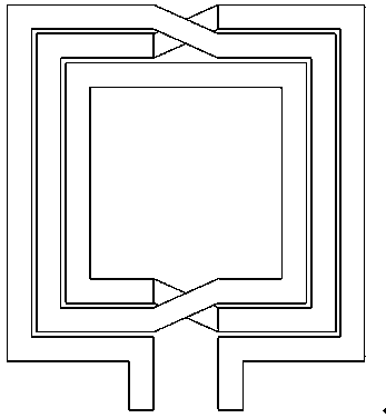
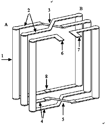
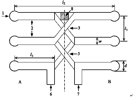
[0015] The technical solution provided by the present invention is: it is composed of horizontal metal lines in the top and bottom metal layers of the silicon substrate and through-silicon holes vertically penetrating the silicon substrate, using the via-first through-silicon hole process Firstly, metal vias are etched in the silicon interposer, and then horizontal interconnect lines are built on the top and back of the silicon interposer and electrically connected to the through silicon vias to form a coil. In order to realize a completely symmetrical structure, there are several groups of crossing wires on the metal lines in the horizontal direction, which are realized by using metal vias and two metal layers.

[0016] The present invention will be described in further detail below in conjunction with the accompanying drawings.

[0017] like figure 2 , 4 As shown, the differential inductor of the present invention includes metal lines in the top and bottom metal layers of...


PUM

PropertyMeasurementUnit
heightaaaaaaaaaa
thicknessaaaaaaaaaa

Abstract

The invention discloses a solenoid type difference inductor based on a silicon through hole. The solenoid type difference inductor is composed of a horizontal metal line which is disposed in the top metal layer and the bottom metal layer of a silicon substrate, and the silicon through hole which vertically penetrates the silicon substrate. By use of a via-first silicon through hole technology, first of all, a metal through hole is etched in a silicon adaptor plate, then a horizontal interconnection line is constructed at the top and the back portion of the silicon adaptor plate, and electrical connection with the silicon through hole is carried out so that a coil is formed. A plurality of intersected lines exist in the metal line in the horizontal direction, and by use of the metal through hole and the two metal layers, a completely symmetrical structure is realized. By using the inductor provided by the invention, the dimension is reduced, and the overall inductance value can be improved at the same time.

Description

technical field [0001] The invention relates to an integrated circuit passive device, in particular to a spiral tube type differential inductor based on silicon through hole technology. Background technique [0002] Silicon-based integrated inductors are one of the important components of radio frequency integrated circuits, and play an important role in circuits such as amplifiers, mixers, and voltage-controlled oscillators. The commonly used silicon-based integrated inductor adopts a planar spiral structure. In the semiconductor process, the winding metal resistance of the spiral inductor is relatively large, and the loss of the silicon-based substrate is high, which makes it difficult to improve the quality factor of the spiral inductor. At the same time, the planar winding The structure occupies a large area, which affects the application of integrated inductors in actual circuits. [0003] The differential structure circuit is the most commonly used circuit design in a...

Claims


Application Information

Patent Timeline
Patent Type & Authority Applications(China)
IPC IPC(8): H01L23/64
CPCH01L2924/0002H01L2924/00
Inventor 唐万春陈如山刘升施永荣王橙黄承沈来伟朱建平
Owner NANJING UNIV OF SCI & TECH
Why Eureka
Try Eureka