Supercharge Your Innovation With Domain-Expert AI Agents!

LED (Light Emitting Diode) chip and manufacturing method thereof

A technology of LED chips and manufacturing methods, which is applied to electrical components, circuits, semiconductor devices, etc., and can solve problems such as reducing efficiency

Inactive Publication Date: 2014-05-28
ENRAYTEK OPTOELECTRONICS
View PDF5 Cites 0 Cited by
  • Summary
  • Abstract
  • Description
  • Claims
  • Application Information

AI Technical Summary

Problems solved by technology

Therefore, only a part of the light generated inside the LED chip can be emitted, which greatly reduces the efficiency of the LED.

Method used


Image

  • LED (Light Emitting Diode) chip and manufacturing method thereof
  • LED (Light Emitting Diode) chip and manufacturing method thereof
  • LED (Light Emitting Diode) chip and manufacturing method thereof

Examples


Embodiment Construction

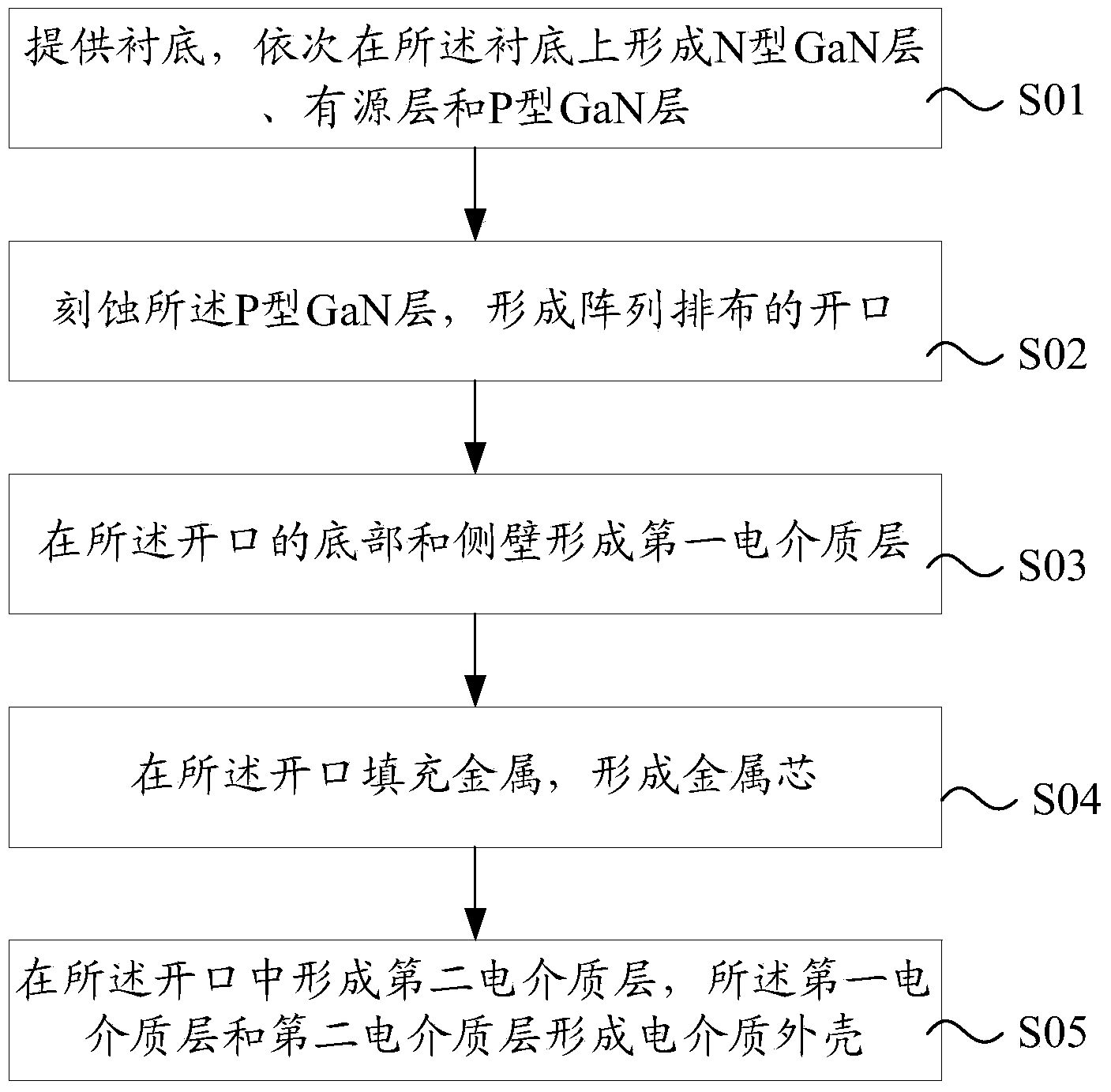
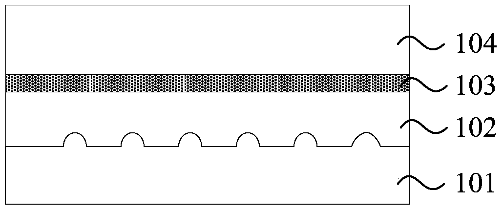
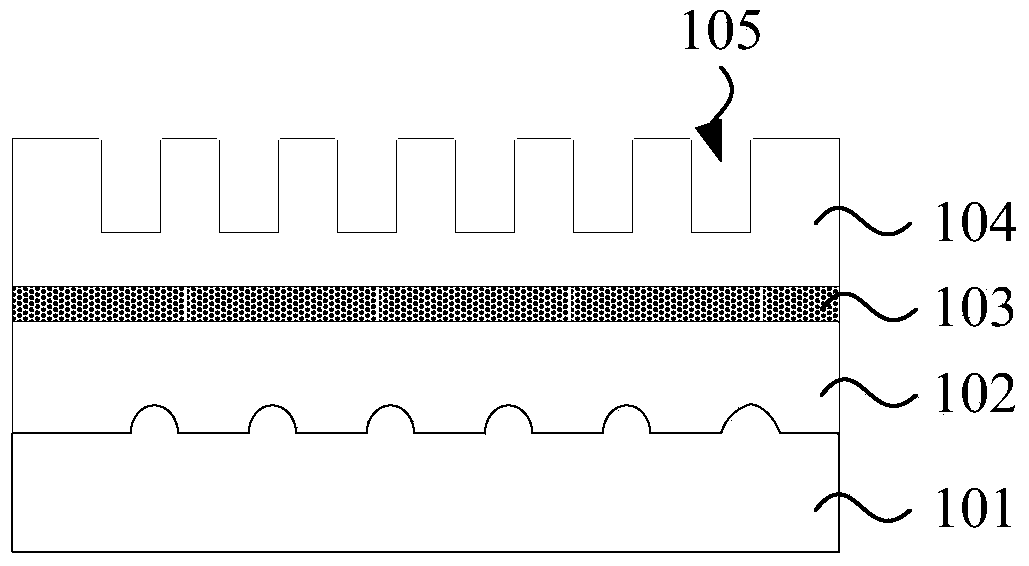
[0034] As mentioned in the background art, improving the luminous efficiency of LED chips is a direction of continuous exploration and improvement in the industry.

[0035] For this reason, the present invention provides a kind of LED chip and its manufacturing method, described LED chip is formed with metal nano-array in P-type GaN layer, and described metal nano-array comprises metal core and dielectric shell, can improve the internal quantum efficiency of LED And light extraction rate, thereby improving the luminous efficiency of LED.

[0036] The present invention will be described in more detail below with reference to the accompanying drawings, wherein preferred embodiments of the present invention are shown, it should be understood that those skilled in the art can modify the present invention described herein and still achieve the advantageous effects of the present invention. Therefore, the following description should be understood as the broad knowledge of those ski...


PUM

PropertyMeasurementUnit
Thicknessaaaaaaaaaa

Abstract

The invention discloses an LED (Light Emitting Diode) chip and a manufacturing method thereof. The LED chip is provided with a metal nanoarray in a P-type GaN layer; the metal nanoarray comprises a metal core and a dielectric medium shell; the metal nanoarray can generate ion resonance with light emitted by an active layer, so that the internal quantum efficiency of an LED is increased; in addition, the light emitted by the active layer can be scattered on the metal nanoarray, so that the light separation rate can be increased, and finally, the light emitting efficiency of the LED can be increased.

Description

technical field [0001] The invention relates to the technical field of LED manufacturing, in particular to an LED chip and a manufacturing method thereof. Background technique [0002] Light Emitting Diode (LED, Light Emitting Diode) is a semiconductor solid-state light-emitting device that uses a semiconductor PN junction as a light-emitting material to convert electricity into light. When a forward voltage is applied to both ends of the semiconductor PN junction, the electrons and holes injected into the PN junction recombine, and the excess energy is released in the form of photons. LED has the advantages of long life and low power consumption. With the maturity of technology, the application fields of LED are becoming more and more diversified, and the requirements for the power and brightness of LED chips are also getting higher and higher. How to increase the power of LED chips It is one of the problems encountered in the development of LED. The power of the LED is c...

Claims


Application Information

Patent Timeline
IPC IPC(8): H01L33/00H01L33/10
CPCH01L33/0062H01L33/0066H01L33/06
Inventor 毕少强
Owner ENRAYTEK OPTOELECTRONICS
Features
  • R&D
  • Intellectual Property
  • Life Sciences
  • Materials
  • Tech Scout
  • Unparalleled Data Quality
  • Higher Quality Content
  • 60% Fewer Hallucinations
Learn More