Optimized dispatching method of photosensitive resistance welding process in multilayer printed circuit board manufacturing

A circuit board manufacturing and photosensitive solder mask technology, applied in the field of intelligent optimal scheduling of production workshops

Inactive Publication Date: 2014-06-04
KUNMING UNIV OF SCI & TECH
View PDF2 Cites 12 Cited by
  • Summary
  • Abstract
  • Description
  • Claims
  • Application Information

AI Technical Summary

Problems solved by technology

[0005] The technical problem to be solved by the present invention is to obtain an excellent solution to the PSR process scheduling problem in a relatively s...

Method used


Image

  • Optimized dispatching method of photosensitive resistance welding process in multilayer printed circuit board manufacturing
  • Optimized dispatching method of photosensitive resistance welding process in multilayer printed circuit board manufacturing
  • Optimized dispatching method of photosensitive resistance welding process in multilayer printed circuit board manufacturing

Examples


Embodiment 1

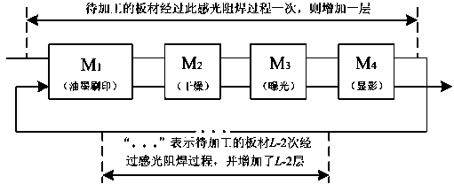
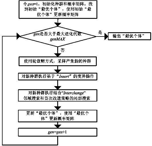
[0084] Embodiment 1: as Figure 1-5 As shown, an optimal scheduling method for the photosensitive solder resist process in the manufacture of multilayer printed circuit boards, by determining the photosensitive solder resist process scheduling model and optimization objectives, and using the optimal scheduling method based on the population incremental learning algorithm to optimize the optimization objectives ; The scheduling model is established according to the processing completion time of each circuit board on each machine, and the optimization goal is to minimize the earliest completion time C max :

[0085]

[0086] In the formula: , , m =4, j =1,..., n x L , k =2,..., m , n x m x L Indicates the size of the problem, n Indicates the total number of circuit board materials to be processed, m Represents the 4 different stages of the photo-solder mask process, L Indicates the number of layers of the circuit board, Represents a collection of positive i...


PUM


Abstract

The invention relates to an optimized dispatching method of the photosensitive resistance welding process in multilayer printed circuit board manufacturing, and belongs to the technical field of intelligent optimized dispatching in a manufacturing shop. According to the optimized dispatching method, a dispatching module and an optimization object in the photosensitive resistance welding process are determined, and an optimized dispatching method based on a population increment learning algorithm is used for optimizing the optimization object; the dispatching module is established according to the processing completed time of all circuit boards on all machines, and meanwhile the optimization object is the minimum earliest completed time. According to the optimized dispatching method of the photosensitive resistance welding process in the multilayer printed circuit board manufacturing, expression of a PSR process is made clear and accurate, a probabilistic model can achieve good balance on precision and complexity, the global search of the algorithm achieves more guidance, the historical information of superior individuals can be effectively utilized, and it is also can be guaranteed that the global search of the algorithm has a certain width, the algorithm can better jump out the local optimum, so that the algorithm can search more regions, the local development capacity of the algorithm is improved, and the quality of a solution can be further improved.

Description

technical field [0001] The invention relates to an optimal scheduling method for a photosensitive solder resist process in the manufacture of multilayer printed circuit boards, and belongs to the technical field of intelligent optimal scheduling of production workshops. Background technique [0002] Printed Circuit Board (PCB) is the carrier for the integration of electronic components and one of the most important components in the electronics industry. Almost every kind of electrical equipment uses printed boards in order to realize the electrical interconnection between different components. In terms of PCB product structure, multilayer boards account for most of the output value, and the manufacturing capacity of multilayer circuit boards has become the most important standard for measuring the technical level of the PCB industry. With the increasingly fierce market competition, how to effectively improve the efficiency of each link in the production process of multilay...

Claims


Application Information

Patent Timeline
IPC IPC(8): G05B19/418
Inventor 钱斌李作成胡蓉孙映白曹高立万婧
Owner KUNMING UNIV OF SCI & TECH
Why Eureka
Try Eureka