Manufacturing method of inductor unit

A manufacturing method and sensor technology, which are used in the manufacture of semiconductor/solid-state devices, electrical components, and electrical solid-state devices, etc., can solve the problems of increased manufacturing difficulty, easy falling off or displacement, and overflowing glue, etc., to ensure reliability, low Crosstalk interference, cost saving effect

Active Publication Date: 2014-06-04
LITE ON SINGAPORE PTE LTD
View PDF5 Cites 10 Cited by
  • Summary
  • Abstract
  • Description
  • Claims
  • Application Information

AI Technical Summary

Problems solved by technology

However, the above-mentioned structure has the following disadvantages: the manufacture and structure of the metal frame are complex; and the packaging structure needs to be glued, and the above-mentioned metal frame is fixed by gluing, but the coating of the glue is not easy to control, too much glue will Causes the problem of overflowing glue; too little glue, the metal frame is not well fixed, easy to

Method used


Image

  • Manufacturing method of inductor unit
  • Manufacturing method of inductor unit
  • Manufacturing method of inductor unit

Examples


Example Embodiment

[0038] The present invention provides a method for manufacturing an inductor unit. The manufacturing method is to achieve the packaging and isolation of the components of the inductor unit by two-time molding and making use of the packaging top plate, which has the effect of reducing the manufacturing cost. It can also solve the shortcomings of traditional assembly methods. The manufacturing method includes the following steps:

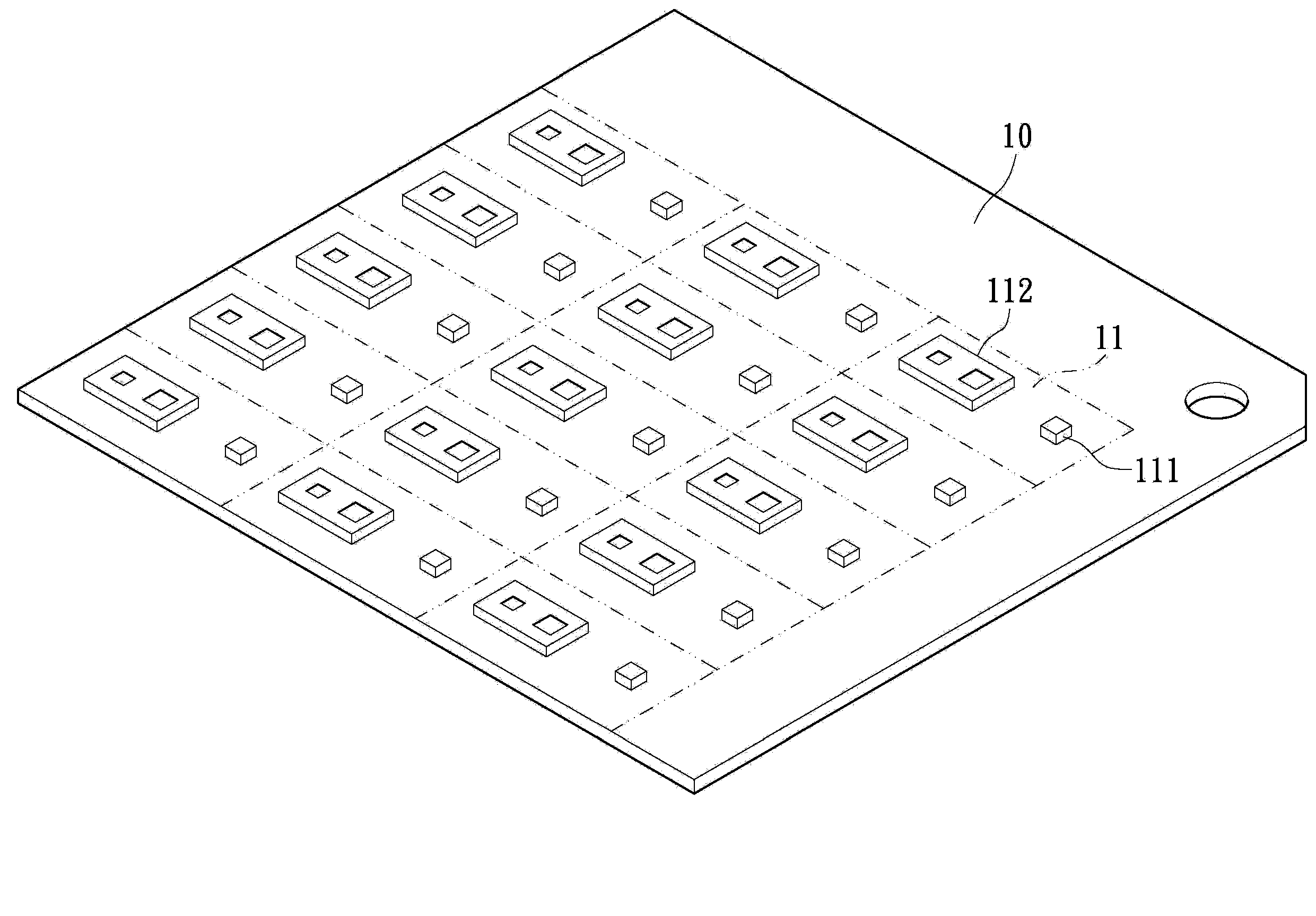
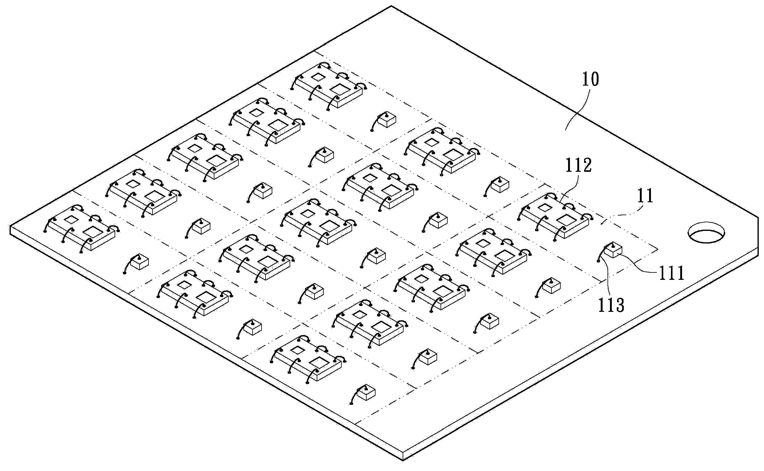
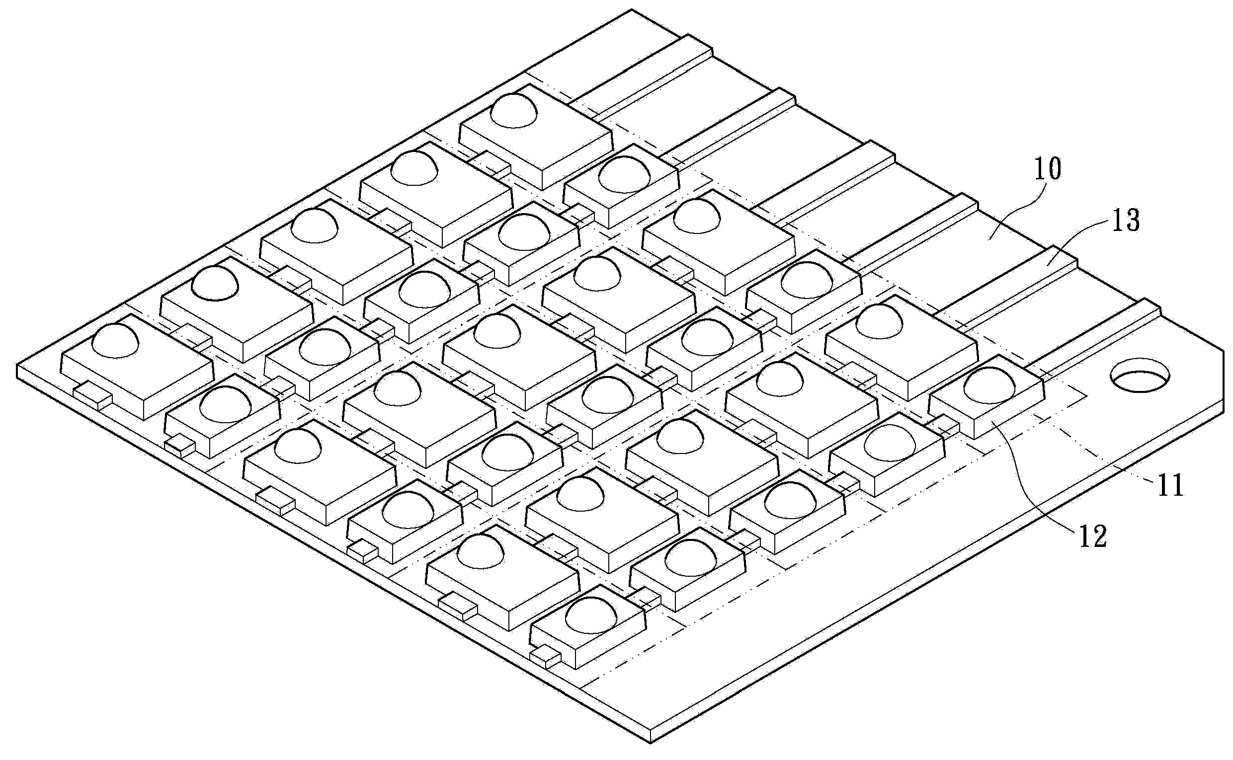
[0039] Please refer to figure 1 As shown, figure 1 The substrate 10, which is the method of manufacturing the sensor unit 1 of the present invention, has a three-dimensional schematic diagram of a signal transmitter 111 and a signal detector 112. First, a substrate 10 is provided, and a plurality of signal transmitters 111 and a plurality of signal detectors 112 are provided, and the plurality of signal transmitters 111 and a plurality of signal detectors 112 are attached to the substrate 10, each of which is The combination of the sensor 111 and the cor...


PUM


Abstract

The invention brings forward a manufacturing method of an inductor unit. The method comprises the following steps: providing a substrate, and attaching multiple signal emitters and multiple signal detectors on the substrate for respectively define multiple inductor areas; then electrically connecting the signal emitters and the signal detectors with the substrate through a wiring bonding mode; carrying out first molding formation manufacturing to enable multiple packaging structures to be molded on the substrate, each packaging structure being corresponding to an inductor area to wrap a signal emitter and a signal detector; providing a packaging top board provided with multiple openings with geometric figures; carrying out second molding formation manufacturing, arranging the packaging top board on the multiple packaging structures, and forming an isolation layer disposed between the packaging board and the substrate through an injection modeling step, the isolation layer wrapping the peripheries of the multiple packaging structures; and finally, performing crystal cutting processing so as to segment each inductor area.

Description

Technical field [0001] The present invention relates to a method for manufacturing an inductor unit, in particular to a method for manufacturing an inductor unit formed by two-time molding and using the production of a package top plate. Background technique [0002] With the development of electronic products, many types of input devices are currently available for operations in electronic systems, such as buttons or keys, mice, trackballs, touch screens, and so on. Recently, the application of touch screens has become more and more common. The touch screen may include a touch panel, which may be a transparent panel with a touch-sensitive surface, so that the work surface covers the viewable area of ​​the display screen. The touch screen allows the user to touch the display screen with a finger or a stylus to make selections and move the cursor, and to achieve corresponding actions according to touch events. The IR proximity sensor is widely used in handheld communication devic...

Claims


Application Information

Patent Timeline
IPC IPC(8): H01L21/56H01L25/16H01L23/31
CPCH01L24/97H01L2224/48091
Inventor 宋广力林生兴吴德财
Owner LITE ON SINGAPORE PTE LTD
Why Eureka
Try Eureka