
Through si via radio frequency test structure and parasitic extracting method thereof

A technology of radio frequency testing and testing structures, which is applied in the direction of single semiconductor device testing, electrical components, electric solid devices, etc. It can solve the problems of difficult removal, multiple de-embedding structures, and large chip area, so as to reduce process costs and improve accuracy. , the effect of small chip area

Active Publication Date: 2014-06-04
SHANGHAI HUAHONG GRACE SEMICON MFG CORP
View PDF4 Cites 8 Cited by
  • Summary
  • Abstract
  • Description
  • Claims
  • Application Information

AI Technical Summary

Problems solved by technology

[0006] The above-mentioned existing structure can extract relatively accurate parasitic inductance and parasitic resistance, but there are also some defects, which lead to certain errors in test results. Two TSVs connected in series will produce mutual inductance, which is difficult to remove, although it can be removed by adding The method of increasing the distance between two TSVs can reduce or eliminate the influence of mutual inductance, but this will also increase the parasitic resistance of the connection part on the back of the two TSVs, and will also increase the area; in addition, from the perspective of de-embedding, this method needs to be equipped with An open circuit structure and a via structure, there are many de-embedding structures, occupying a large area of ​​the chip, and the cost is high

Method used


Image

  • Through si via radio frequency test structure and parasitic extracting method thereof
  • Through si via radio frequency test structure and parasitic extracting method thereof
  • Through si via radio frequency test structure and parasitic extracting method thereof

Examples


Embodiment Construction

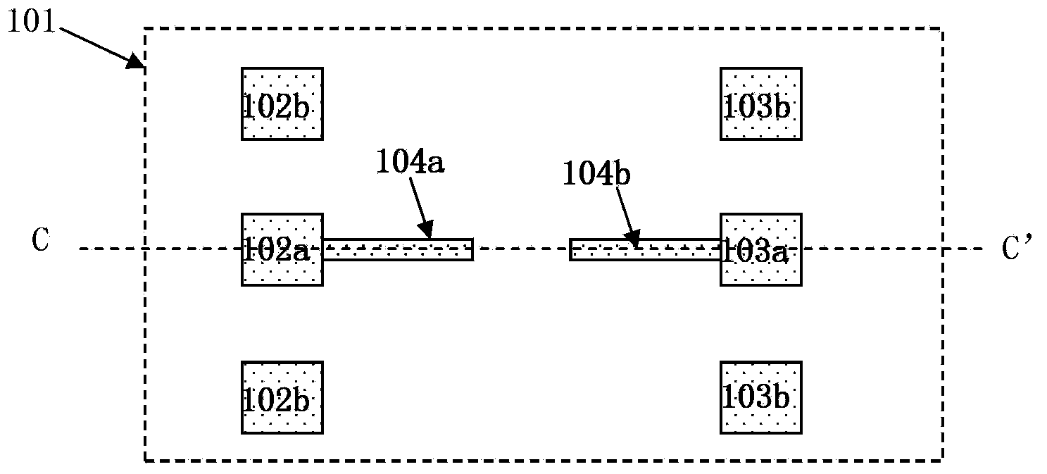
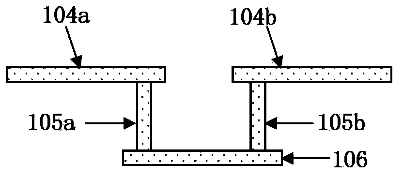
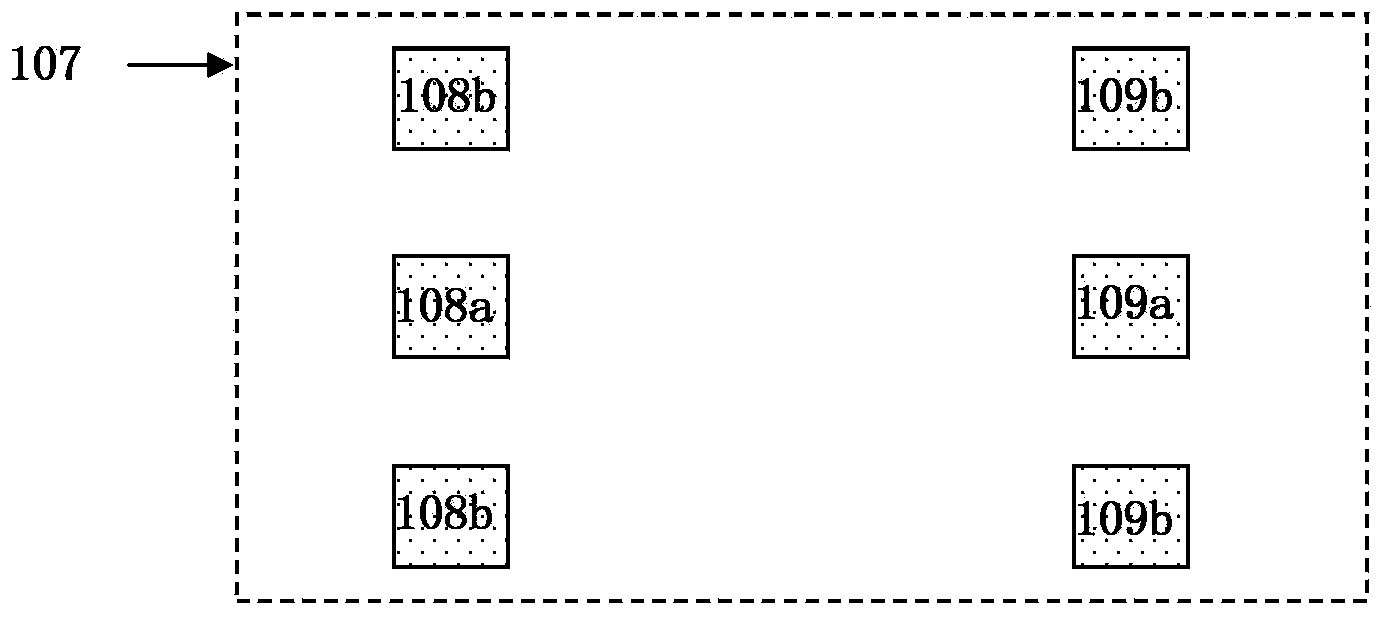
[0032] Such as Figure 2A As shown, it is a top view of the test structure 1 of the radio frequency test structure of the through-silicon via in the embodiment of the present invention; Figure 2B shown, is along the Figure 2A The profile of the line AA' in Figure 2C shown, is along the Figure 2A The section view of the BB' line in ; such as Figure 2D As shown, it is a top view of the open circuit de-embedding structure 2 of the radio frequency test structure of the TSV according to the embodiment of the present invention. The radio frequency test structure of the TSV in the embodiment of the present invention is composed of a test structure one 1 and an open circuit de-embedding structure two 8 .

[0033] The test structure 1 includes port 1 and port 2. The port 1 is composed of a signal terminal 2a and two ground terminals 2b in a ground-signal-ground (GSG) structure; the port 2 is composed of a signal terminal 3a It is composed of two ground terminals 3b in a groun...


PUM


Abstract

The invention discloses a through si via radio frequency test structure which is formed by a first test structure and a second open circuit de-embedding structure. The first test structure comprises a first port and a second port of a GSG bonding pad structure; signal ends of the first port and the second port are connected in a short circuit manner by a first top metal; a tested through si via is arranged between signal ends of the first port and the second port; the top of the tested through si via is connected with the first top metal; the bottom of tested through si via is connected with a second back metal; and grounding terminals of the first port and the second port are respectively connected with the second back metal through a grounding through si via array. The second open circuit de-embedding structure and the first test structure, after the first top metal and tested through si via are removed, are the same in structure. The invention also discloses a parasitic extracting method of the through si via radio frequency test structure. According to the invention, the accuracy of testing the parasitic resistance and inductance of the through si via can be improved, and the test structure area and the process cost can be reduced.

Description

technical field [0001] The invention relates to the field of semiconductor integrated circuit manufacturing, in particular to a radio frequency testing structure of through-silicon holes. The invention also relates to a parasitic extraction method of the radio frequency test structure of the through-silicon hole. Background technique [0002] The Through Silicon Via (TSV) process is an emerging integrated circuit manufacturing process. The circuit fabricated on the upper surface of the silicon wafer is connected to the back of the silicon wafer through the metal filled in the silicon via. Combined with the three-dimensional packaging process, it makes IC layout has evolved from traditional two-dimensional side-by-side arrangement to more advanced three-dimensional stacking, so that component packaging is more compact, and by shortening the distance between chip leads, the frequency characteristics and power characteristics of the circuit can be greatly improved. The through...

Claims


Application Information

Patent Timeline
IPC IPC(8): H01L23/544G01R31/26
Inventor 黄景丰
Owner SHANGHAI HUAHONG GRACE SEMICON MFG CORP
Learn More