Power-supply clamp ESD circuit

A power supply voltage and clamping technology, which is applied in the direction of circuit devices, emergency protection circuit devices, emergency protection circuit devices for limiting overcurrent/overvoltage, etc. Discharge circuit conduction and other problems, to achieve the effect of ensuring reliability, increasing reliability and good reliability

Inactive Publication Date: 2014-06-04
SHANGHAI HUAHONG INTEGRATED CIRCUIT
View PDF4 Cites 8 Cited by
  • Summary
  • Abstract
  • Description
  • Claims
  • Application Information

AI Technical Summary

Problems solved by technology

However, in the 0.13μm or smaller process, the power supply voltage is relatively low, which will cause the state of the inverter INV1 to be confused and affect the normal operation of the chip.
[0009] When the chip is working normally, the input terminal of the inverter INV1 is at a high level, but the actual voltage value is the power supply voltage minus a threshold voltage, which will cause the inverter INV1 to be in a semi-conducting or critical conducting state, and the leakage The discharge circuit may be turned on, which will affect the normal operation of the chip

Method used


Image

  • Power-supply clamp ESD circuit
  • Power-supply clamp ESD circuit

Examples


Embodiment Construction

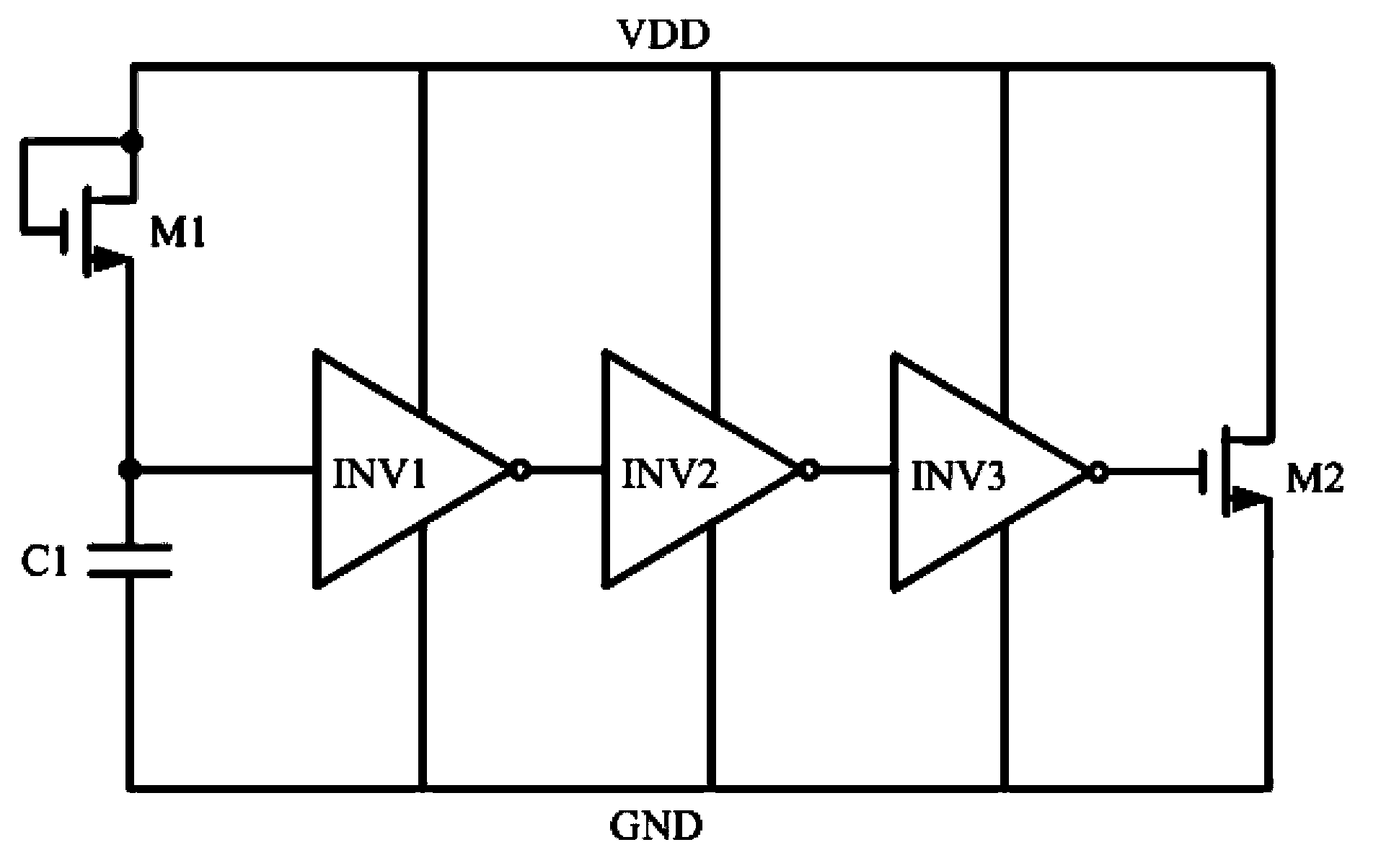
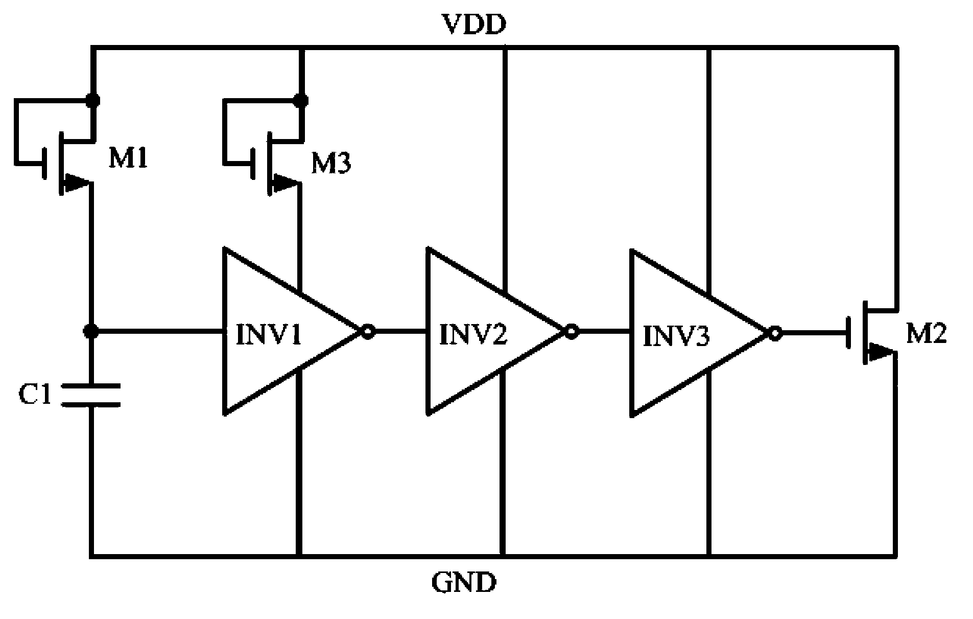
[0020] see figure 2 As shown, in the following embodiments, the power clamp ESD circuit of the present invention includes:

[0021] A detection circuit is composed of a first NMOS transistor M1 and a capacitor. The first NMOS transistor M1 is diode-connected, its gate and drain are connected to the power supply voltage VDD, its source is connected to one end of the capacitor C1, and the other end of the capacitor C1 is grounded to GND.

[0022] A buffer circuit is composed of three series-connected inverters INV1-INV3, wherein the input terminal of the first inverter INV1 is connected to the source of the first NMOS transistor M1 and the connection terminal of the capacitor C1. A diode-connected third NMOS transistor M3 is connected in series between the power supply terminal of the first inverter INV1 and the power supply voltage VDD.

[0023] A discharge circuit is composed of a second NMOS transistor M2, the gate of which is connected to the output terminal of the third ...


PUM


Abstract

The invention discloses a power-supply clamp ESD circuit which includes a detection circuit, a buffer circuit and a leakage circuit. The buffer circuit includes a phase inverter, or three serially-connected phase inverters or five serially-connected phase inverters. A connection wire of a power-supply end of a first phase inverter in the buffer circuit and a power-supply voltage is connected serially with an NMOS transistor which is connected with a diode, that is, a grid electrode and a drain electrode of the NMOS transistor are connected with the power-supply voltage and a source electrode of the NMOS transistor is connected with the power-supply end of the first phase inverter. The power-supply clamp ESD circuit is capable of ensuring that the ESD circuit is in a closed state and does not affect the normal work of a chip when the chip works normally.

Description

technical field [0001] The invention relates to the field of ESD (electrostatic discharge) protection, in particular to a power clamp ESD circuit. Background technique [0002] In recent years, with the rapid development of integrated circuit technology, the line width of MOS transistors has become narrower and narrower, the junction depth has become shallower and shallower, and the thickness of the gate oxide layer has become thinner and thinner, all of which have accelerated the demand for ESD in circuit design . When the line width is 1 μm, ESD events have little impact on the circuit. When entering the era of 0.18 μm and 0.13 μm, especially the era below 90 nanometers, ESD has become an urgent problem. [0003] Common ESD is divided into HBM (Human body model) mode, MM (machine model) mode and CDM (Charged device model) mode. The HBM and MM modes discharge the chip externally. It is not enough to rely solely on the ESD protection circuit of the input and output ports. ...

Claims


Application Information

Patent Timeline
Patent Type & Authority Applications(China)
IPC IPC(8): H02H9/00H02H9/04
Inventor 马和良赵英瑞
Owner SHANGHAI HUAHONG INTEGRATED CIRCUIT
Why Eureka
Try Eureka