Printed circuit board and method of manufacturing thereof

A technology for printed circuit substrates and manufacturing methods, which is applied in the fields of printed circuit manufacturing, printed circuits, printed circuits, etc., can solve problems such as not being able to adapt to the trend of miniaturization, achieve the effect of improving product quality and performance, and reducing board bending deformation

Inactive Publication Date: 2014-06-04
DAEDUCK GDS
View PDF5 Cites 1 Cited by
  • Summary
  • Abstract
  • Description
  • Claims
  • Application Information

AI Technical Summary

Problems solved by technology

[0008] In order to prevent the substrate from bending and deforming, the thickness of the printed circuit substrate can be increased during manufacturing, but this does not meet the trend of miniaturization

Method used


Image

  • Printed circuit board and method of manufacturing thereof
  • Printed circuit board and method of manufacturing thereof
  • Printed circuit board and method of manufacturing thereof

Examples


Embodiment Construction

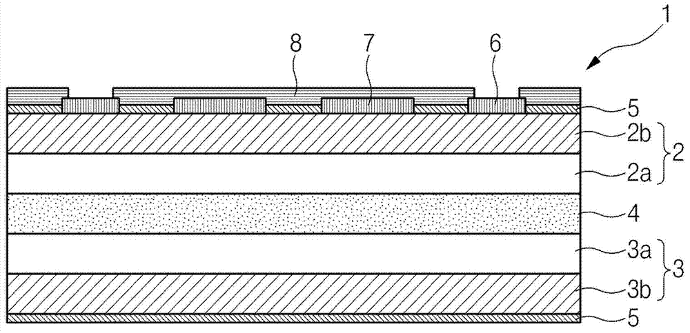
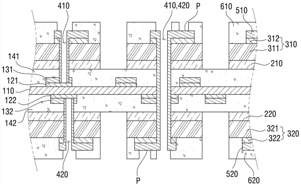
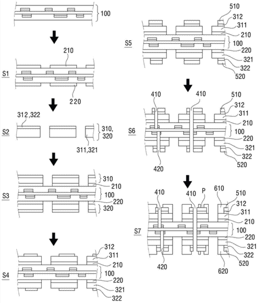
[0056] figure 1 is a cross-sectional structure diagram illustrating a conventional printed circuit board; figure 2 is a cross-sectional structure diagram illustrating a printed circuit board according to an embodiment of the present invention; image 3 is a manufacturing process diagram illustrating a printed circuit board according to an embodiment of the present invention; Figure 4a It is a comparison chart illustrating the amount of SMD front and rear inclination of the printed circuit board according to the embodiment of the present invention; Figure 4b It is a comparison chart illustrating the amount of SMD front and rear inclination of a conventional printed circuit board; Figure 5 It is a comparison graph showing the flexural strength of a printed circuit board according to an embodiment of the present invention and a printed circuit board of the prior art.

[0057] Such as Figure 2 to Figure 3 As shown, the printed circuit board according to the embodiment of ...


PUM

PropertyMeasurementUnit
thicknessaaaaaaaaaa
thicknessaaaaaaaaaa
thicknessaaaaaaaaaa

Abstract

A printed circuit board and a manufacturing method thereof are provided to improve quality or performance of a product by minimizing deformation by heat while a part such as a camera module and et cetera is being mounted. A printed circuit board includes an internal layer (100), an external insulation layer and an external core layer. The internal layer is made of a flexible circuit board. The external insulation layer is laminated on more than one layer of one or the other layer. The external core layer is laminated on the external insulation layer and includes a reinforcement layer made of a rigid material of which strength is greater than the internal layer and external layer. The second external core layer includes a second reinforcement layer and a second external circuit layer. The first reinforcement layer and the second reinforcement layer are made of at least one material among FR-4, HI-tg or BT.

Description

technical field [0001] The invention relates to a printed circuit substrate and its manufacturing method, especially a printed circuit substrate with rigid material added to maintain flatness when installing a camera module and its manufacturing method. Background technique [0002] figure 1 It is a cross-sectional structural view of a conventional printed circuit board. Such as figure 1 As shown, the printed circuit substrate 1 of the prior art includes an upper base layer 2 and a lower base layer 3, and the upper base layer 2 and the lower base layer 3 are bonded together by an adhesive film 4; The first insulating layer film 2a on the side and the first copper foil layer 2b for forming circuit patterns that are thermally pressed on the first insulating layer film 2a; the lower base layer 3 includes the second layer laminated on the other side of the adhesive film 4 The insulating layer film 3a and the second insulating layer film 3b are thermally pressed on the outside...

Claims


Application Information

Patent Timeline
Patent Type & Authority Applications(China)
IPC IPC(8): H05K1/02H05K3/46
CPCH05K1/0271H05K1/09H05K3/0023H05K3/022H05K3/241H05K3/4602H05K2201/0154
Inventor 黄晶淏申允铁李忠植
Owner DAEDUCK GDS
Why Eureka
Try Eureka