Electroplating device and method of plating copper in via hole of PCB (Printed Circuit Board)

An electroplating device and via hole technology, applied in the direction of electrical components, electrolytic process, electrolytic components, etc., can solve the problems of difficult to achieve the required hole copper thickness, difficult, difficult processing, etc., to ensure the effect of electroplating, easy to realize, Easy to adjust the effect

Inactive Publication Date: 2014-06-11
PEKING UNIV FOUNDER GRP CO LTD +1
View PDF6 Cites 5 Cited by
  • Summary
  • Abstract
  • Description
  • Claims
  • Application Information

AI Technical Summary

Problems solved by technology

However, for the production of ultra-high aspect ratio and fine circuit PCB boards, there is a contradiction between the surface copper thickness and hole copper thickness requirements.
In the production process of PCB boards with ultra-high thickness-to-diameter ratio, thin lines, small spacing, and fine lines, there are certain requirements for the surface copper thickness of the circuit board. There is also a minimum thickness requirement for the hole copper thickness of the via hole, which leads to a contradiction between the surface copper thickness requirement and the hole copper thickness requirement, which brings difficulties to the processing and production; at the same time, the via hole with a small aperture is very difficult for ordinary electroplating. Difficult to achieve the required hole copper thickness
There is a bottleneck in the conventional PCB board manufacturing method, and it is difficult or even impossible to manufacture a PCB board with ultra-high thickness-to-diameter ratio and fine lines

Method used


Image

  • Electroplating device and method of plating copper in via hole of PCB (Printed Circuit Board)
  • Electroplating device and method of plating copper in via hole of PCB (Printed Circuit Board)
  • Electroplating device and method of plating copper in via hole of PCB (Printed Circuit Board)

Examples


Embodiment Construction

[0071] In order to understand the above-mentioned purpose, features and advantages of the present invention more clearly, the present invention will be further described in detail below in conjunction with the accompanying drawings and specific embodiments. It should be noted that, in the case of no conflict, the embodiments of the present application and the features in the embodiments can be combined with each other.

[0072] In the following description, many specific details are set forth in order to fully understand the present invention. However, the present invention can also be implemented in other ways than described here. Therefore, the protection scope of the present invention is not limited by the specific implementation disclosed below. Example limitations.

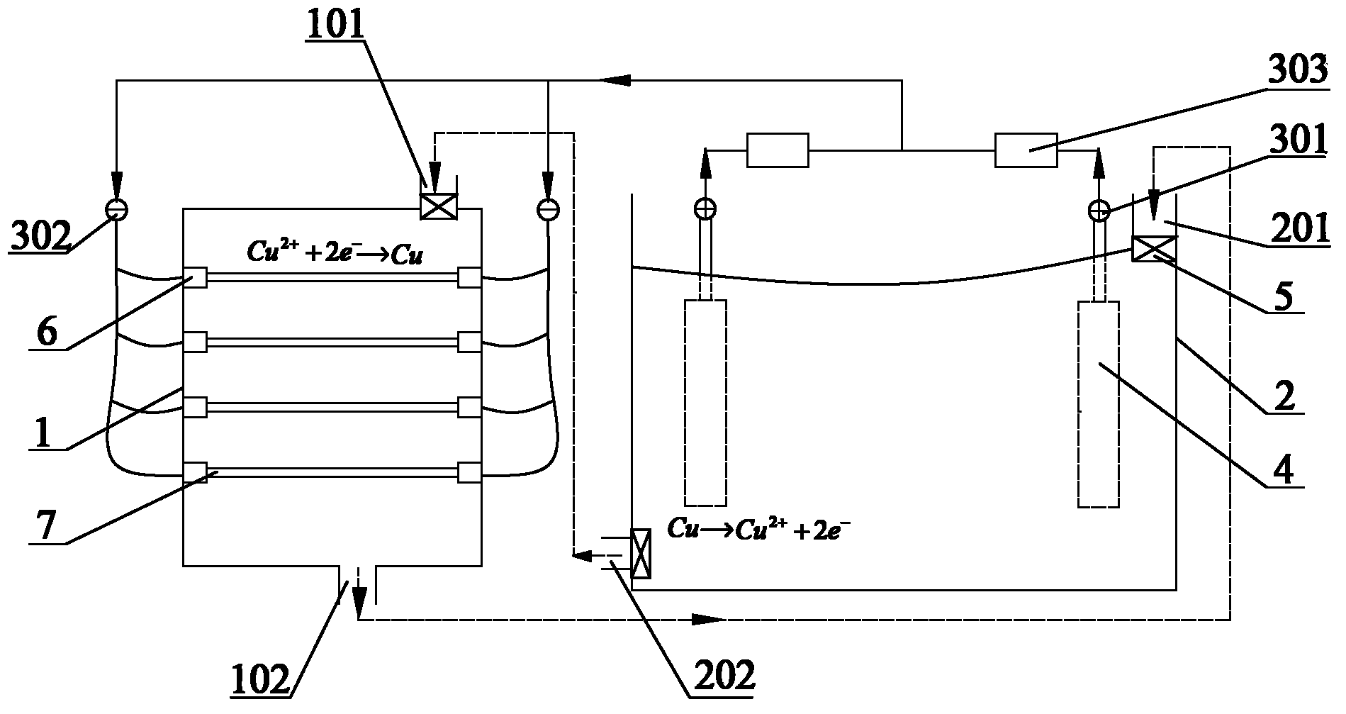
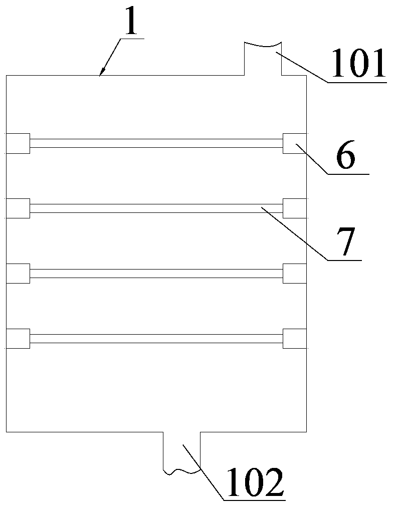
[0073] Such as figure 2 As shown, the present invention provides an electroplating device, including an electroplating tank 1 and a secondary tank 2, the anode metal 4 in the secondary tank 2 is connected t...


PUM


Abstract

The invention provides an electroplating device which comprises an electroplating bath and an auxiliary bath, wherein the anodic metal in the auxiliary bath is connected to a power supply device, a to-be-electroplated workpiece is connected to the cathode of the power supply device, the auxiliary bath is communicated with the electroplating bath and provides an electroplate liquid to the electroplating bath, the anodic metal immerges into the electroplate liquid, and the electroplating bath is used for plating metal to the to-be-electroplated workpiece. The invention further provides a method of plating copper into a via hole of a PCB (Printed Circuit Board). The electroplating device provided by the invention can electroplate PCBs with super ratio of thickness to radial dimension and fine lines.

Description

technical field [0001] The invention relates to the field of circuit board processing, in particular to an electroplating device and a copper plating method for through holes of a PCB board. Background technique [0002] With the rapid development of electronic products, PCB (Printed Circulate Board, printed circuit board) board, as its main component, is also advancing in the direction of high density, high level and multifunctionality, and the thickness and number of layers of PCB board are increasing. The aperture tends to be smaller, and the aspect ratio of the circuit board (the ratio of the thickness of the PCB to the aperture of the via hole on the PCB) rises linearly. As a result, PCB boards have entered the era of ultra-high aspect ratio and fine lines. Ultra-high aspect ratio generally means that the ratio of the thickness of the circuit board to the diameter of the via hole is greater than 12:1, and even reaches 20:1. [0003] In the conventional PCB board manuf...

Claims


Application Information

Patent Timeline
Patent Type & Authority Applications(China)
IPC IPC(8): C25D7/00C25D17/00C25D21/06H05K3/18H05K3/42
Inventor 谢海山李华华何勤刘光来
Owner PEKING UNIV FOUNDER GRP CO LTD
Why Eureka
Try Eureka