Etching method and device for improving side wall streaks
A streak and process technology, applied in the field of etching process and its devices, can solve the problems of polymer sidewall streaks, high DC bias, polymer weight, etc., and achieve the effect of improving the streaks of through holes
- Summary
- Abstract
- Description
- Claims
- Application Information
AI Technical Summary
Problems solved by technology
Method used
Image
Examples
Embodiment 1
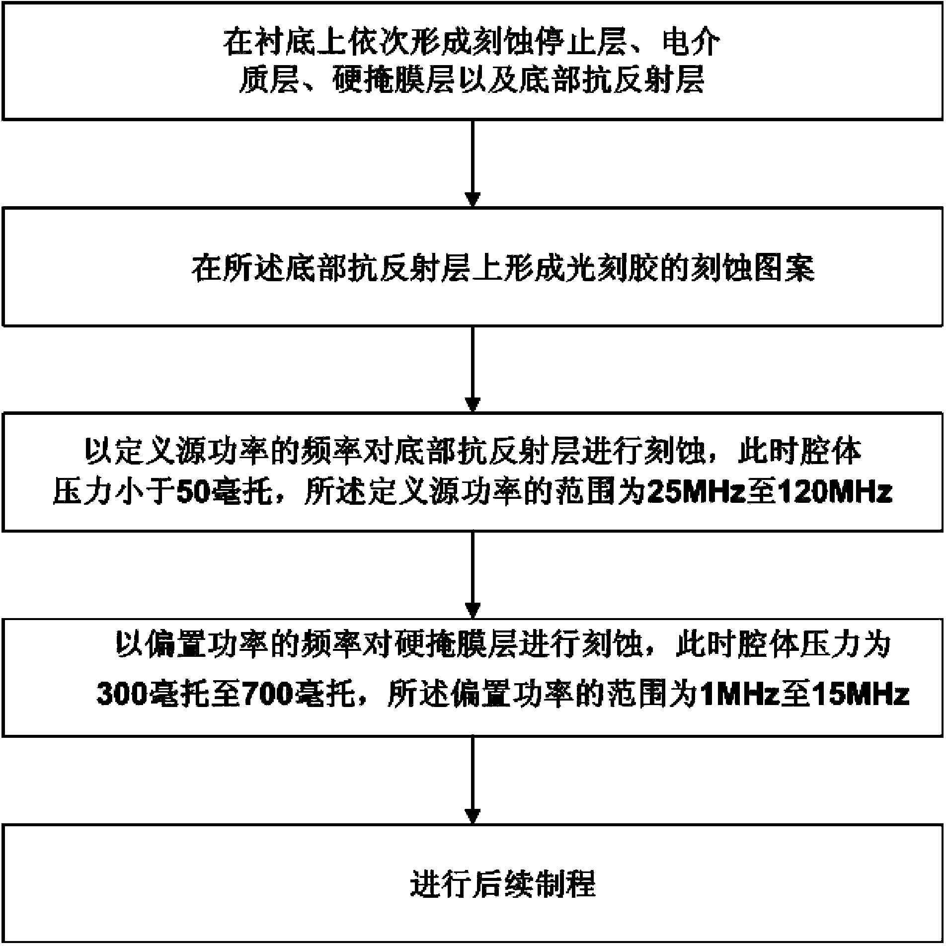
[0076] Using the etching process and device for improving sidewall streaks of the present invention to etch the bottom dielectric isolation layer includes the following specific steps:
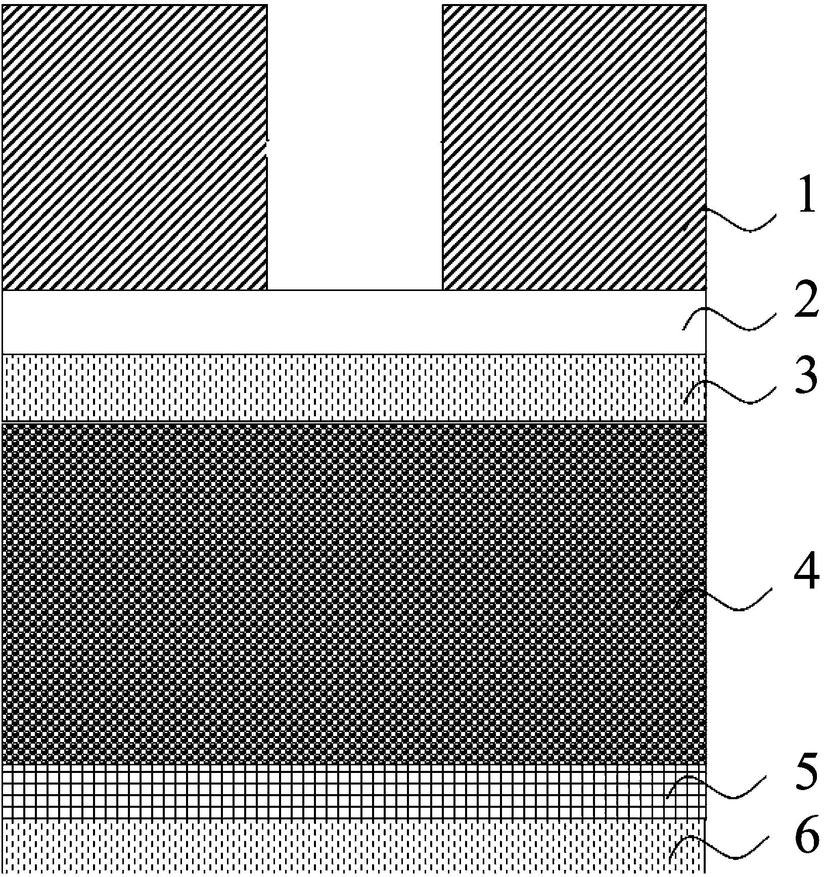
[0077] The substrate is placed on the pedestal in the plasma reaction chamber, and an etching stop layer, a dielectric layer, a hard mask layer and a bottom anti-reflection layer are sequentially formed on the substrate.
[0078] An etching pattern of photoresist is formed on the bottom anti-reflection layer.
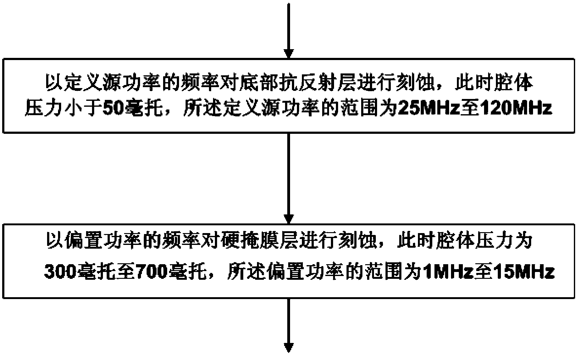
[0079] The plasma generator in the plasma reaction chamber etches the bottom anti-reflection layer at a frequency that defines the source power. At this time, the chamber pressure is 45 mTorr, and the mixed gas introduced during the etching of the bottom anti-reflection layer includes: N 2 and CO 2 The mixed gas, the defined source power is 60MHz.
[0080] Then the plasma generator etches the hard mask layer at the frequency of the bias power, and the cavity pressure is 600 millitorr ...
Embodiment 2
[0084] Using the etching process and device for improving sidewall streaks of the present invention to etch the bottom dielectric isolation layer includes the following specific steps:
[0085] The substrate is placed on the pedestal in the plasma reaction chamber, and an etching stop layer, a dielectric layer, a hard mask layer and a bottom anti-reflection layer are sequentially formed on the substrate.
[0086] An etching pattern of photoresist is formed on the bottom anti-reflection layer.
[0087] The plasma generator in the plasma reaction chamber etches the bottom anti-reflection layer at a frequency that defines the source power. At this time, the chamber pressure is 40 mTorr, and the mixed gas introduced during the etching of the bottom anti-reflection layer includes: N 2 and O 2 The mixed gas, the defined source power is 70MHz.
[0088] Then the plasma generator etches the hard mask layer at the frequency of the bias power. At this time, the chamber pressure is 500 ...
Embodiment 3
[0092] Using the etching process and device for improving sidewall streaks of the present invention to etch the bottom dielectric isolation layer includes the following specific steps:
[0093] The substrate is placed on the pedestal in the plasma reaction chamber, and an etching stop layer, a dielectric layer, a hard mask layer and a bottom anti-reflection layer are sequentially formed on the substrate.
[0094] An etching pattern of photoresist is formed on the bottom anti-reflection layer.
[0095] The plasma generator in the plasma reaction chamber etches the bottom anti-reflection layer at a frequency that defines the source power. At this time, the chamber pressure is 35 mTorr, and the mixed gas introduced during the etching of the bottom anti-reflection layer includes: N 2 and CO 2 The mixed gas, the defined source power is 65MHz.
[0096] Then the plasma generator etches the hard mask layer at the frequency of the bias power. At this time, the chamber pressure is 550...
PUM
 Abstract
Description
Claims
Application Information


