
Sensor for active leveling detection of nanoimprint lithography working tables

A detection sensor and nano-imprinting technology, which is applied in the direction of instruments, measuring devices, and optical devices, can solve the problems of high installation and positioning accuracy, difficult implementation, and increased cost of active-adjustable nano-imprinting workbenches. Achieve the effects of eliminating system errors, saving installation and adjustment workload, and reducing manufacturing and testing costs

Inactive Publication Date: 2014-06-18
XI AN JIAOTONG UNIV
View PDF8 Cites 12 Cited by
  • Summary
  • Abstract
  • Description
  • Claims
  • Application Information

AI Technical Summary

Problems solved by technology

The use of three high-precision displacement sensors as the detection method for the parallelism of two planes has the following two shortcomings: (1) The installation and positioning accuracy of the three displacement sensors is very high, and it needs to be higher than the distance between the planes to be tested. It is very difficult to implement position calibration and calibration of a pair of parallel planes with an order of magnitude of parallelism; (2) using three displacement sensors for detection at the same time greatly increases the cost of the active adjustment nanoimprinting workbench

Method used


Image

  • Sensor for active leveling detection of nanoimprint lithography working tables
  • Sensor for active leveling detection of nanoimprint lithography working tables
  • Sensor for active leveling detection of nanoimprint lithography working tables

Examples


Embodiment Construction

[0021] The present invention will be described in detail below in conjunction with the accompanying drawings.

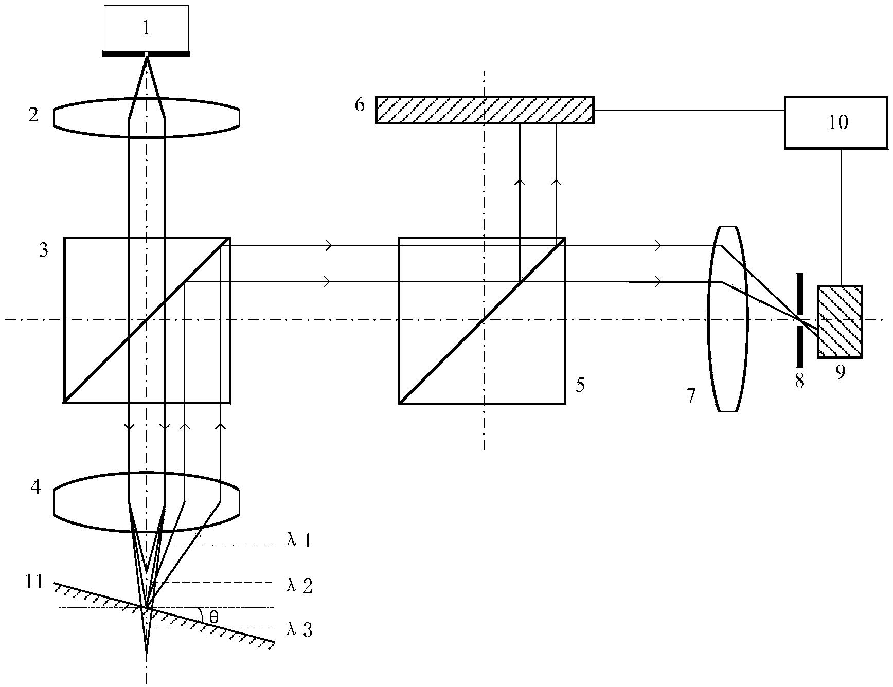
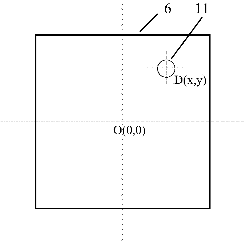
[0022] refer to figure 1 , an active leveling detection sensor for a nanoimprint worktable, including a broadband point light source 1, the light emitted by the broadband point light source 1 passes through the first achromatic beam expander and collimator optical lens 2 to form a broadband parallel beam, and the light of different wavelengths There is no phase difference; the parallel light enters the dispersion lens group 4 after passing through the first dichroic prism 3, and the light of different wavelengths produces spectral dispersion, forming a series of focal points in space; a certain monochromatic light focused on the surface of an inclined object passes through the substrate 11 Reflected by the dispersive lens group 4, the outgoing parallel monochromatic light beam is equal to the incident light and has an optical axis offset; the monochromatic parallel l...


PUM


Abstract

The invention discloses a sensor for active leveling detection of nanoimprint lithography working tables. According to the sensor for active leveling detection of the nanoimprint lithography working tables, light emitted by a bandwidth point light source forms parallel bandwidth light beams after passing through a first color-difference-free beam-expanding collimating optical lens, the parallel light beams enter a dispersing lens set after passing through a first beam splitter prism, and thus a series of focus points are formed in the space; certain monochromatic light focused on the surface of an oblique object passes through the dispersing lens set through the reflection of a substrate, and parallel monochromatic light beams are emitted, wherein the diameter of each monochromatic light beam is equal to the diameter of incident light, and the optical axes of the monochromatic light beams deviate; the parallel monochromatic light beams are divided into two parts after being reflected by the first beam splitter prism and a second beam splitter prism, and one part of the parallel monochromatic light beams reach a two-dimensional photoelectric position detector; the other part of the parallel monochromatic light beams are focused through a second color-difference-free optical lens and are received by a spectrum detector after being subject to pinhole filtering, deviation of the degree of parallelism between working surfaces of the working tables is detected through the two-dimensional photoelectric position detector, and the distance between the working surfaces of the working tables is detected through the spectrum detector. The sensor for active leveling detection of the nanoimprint lithography working tables has the advantages of being low in production cost, reliable in installation and easy to operate.

Description

technical field [0001] The invention belongs to the technical field of micro-nano manufacturing and optical precision measurement, and in particular relates to a sensor for active leveling detection of a nano-imprint working platform. technical background [0002] Nano-Imprint Lithography (NIL) is a micro-nano-fabrication technology that uses a template to achieve patterning through the force deformation of the resist on the substrate. Compared with other micro-nano manufacturing methods, NIL has the characteristics of high resolution, low cost and high productivity, and can be applied to integrated circuits, biomedical products, ultra-high-density disks, optical components, organic electronics, molecular electronics, etc. Field, known as one of the top ten technologies that can change the world. [0003] The nanoimprint process requires that the parallelism between the template and the substrate be ensured so that the template and the substrate can be in uniform contact. ...

Claims


Application Information

Patent Timeline
IPC IPC(8): G01B11/14G01B11/26
Inventor 丁玉成邵金友王春慧刘京昀
Owner XI AN JIAOTONG UNIV
Features
  • Generate Ideas
  • Intellectual Property
  • Life Sciences
  • Materials
  • Tech Scout
  • Unparalleled Data Quality
  • Higher Quality Content
  • 60% Fewer Hallucinations
Learn More