
System and method for performing SRAM write assist

A technology of write assistance and bit lines, applied in the field of write assistance, can solve the problem that SRAM storage elements cannot be written reliably

Inactive Publication Date: 2014-06-18
NVIDIA CORP
View PDF3 Cites 7 Cited by
  • Summary
  • Abstract
  • Description
  • Claims
  • Application Information

AI Technical Summary

Problems solved by technology

As a result, SRAM cells cannot be reliably written to

Method used


Image

  • System and method for performing SRAM write assist
  • System and method for performing SRAM write assist
  • System and method for performing SRAM write assist

Examples


Embodiment Construction

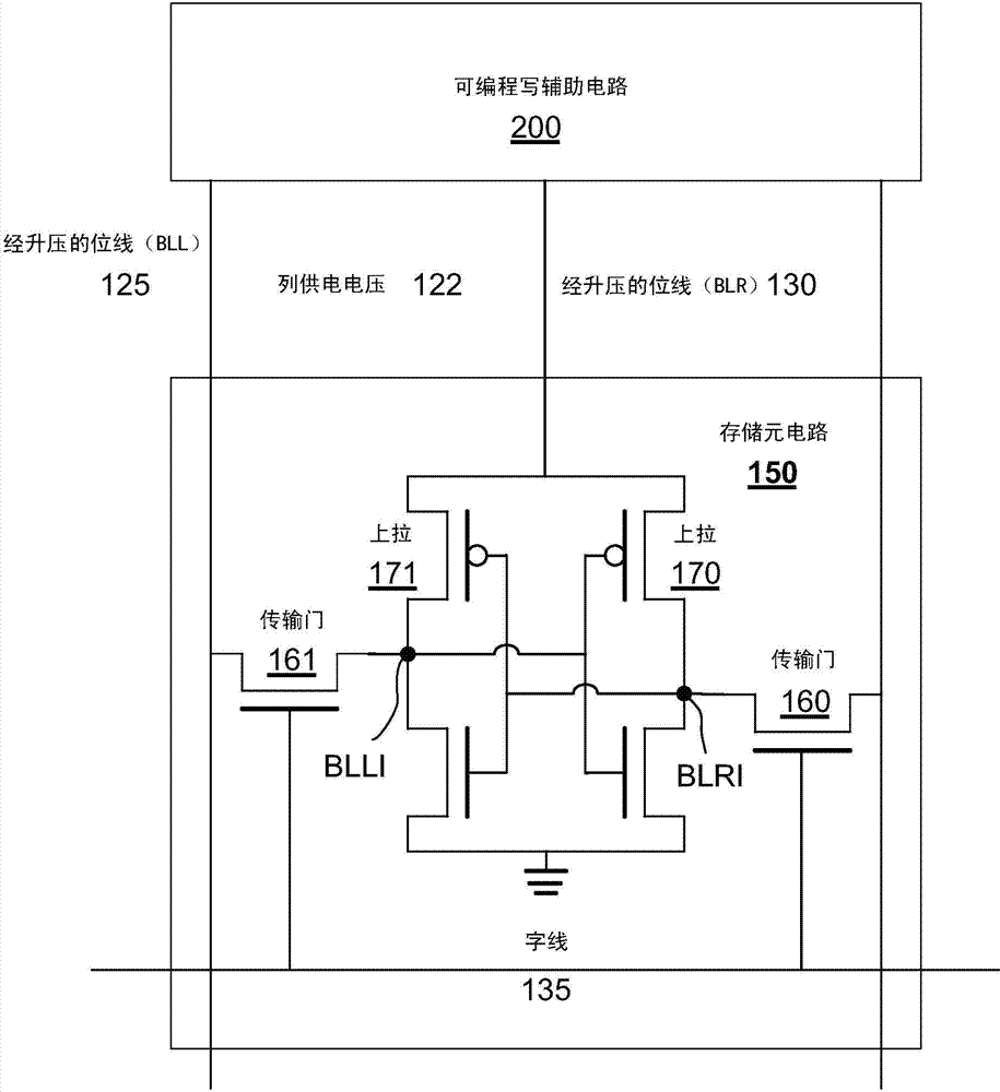
[0015] As previously explained, changes in circuit characteristics can strengthen the PMOS pull-up transistors and weaken the NMOS transmission gates of the memory elements, making the memory cells unreliably writable. Unfortunately, changing the size of the PMOS pull-up transistors to weaken the PMOS pull-ups and changing the size of the NMOS pass-gate transistors to strengthen the NMOS pass-gates is not an effective technique for improving write reliability. For example, when a memory cell is implemented using a Fin-FET (Fin-FET), the size of the memory cell is quantified based on the number of fins. This means that for various design reasons, transistor sizing is not an effective technique for improving write reliability even with minimal changes in circuit characteristics. The write assist weakens the PMOS pull-up transistor and strengthens the NMOS pass gate to improve write reliability without relying on changing the size of the transistor. Write assist is enabled durin...


PUM


Abstract

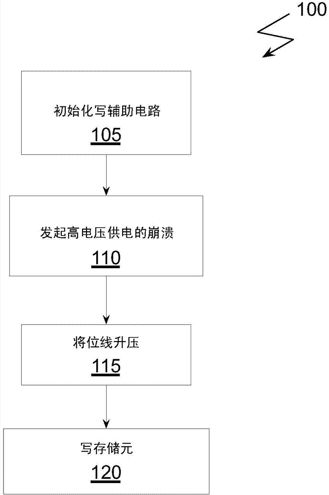
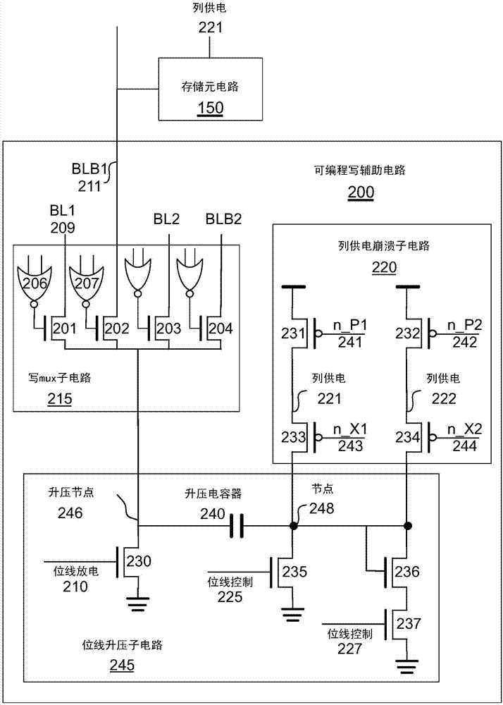
A method and a system are provided for performing write assist. Write assist circuitry is initialized and voltage collapse is initiated to reduce a column supply voltage provided to a storage cell. A bitline of the storage cell is boosted to a boosted voltage level that is below a low supply voltage provided to the storage cell and data encoded by the bitline is written to the storage cell.

Description

technical field [0001] The present invention relates to memory circuits, and more particularly, to write assist. Background technique [0002] Reducing the operating supply voltage (Vmin) is an effective strategy for improving the energy efficiency of integrated circuits. However, write operations to static random access memory (SRAM) cells at lower operating supply voltages due to variations in circuit characteristics such as threshold voltages due to manufacturing processes and / or age of integrated circuit devices may become unreliable. [0003] To write to a conventional 6-transistor memory cell, the data to be written is encoded as differential values ​​on the bit lines (BL and BLB). For example, data=0 is encoded as BL=0 and BLB=1, and data=1 is encoded as BL=1 and BLB=0, where 1 (true) is a high voltage level and 0 (false) is a low voltage level. When the word line is enabled, NMOS (N-type metal oxide semiconductor) transistor pass gates that couple the bit line pa...

Claims


Application Information

Patent Timeline
IPC IPC(8): G11C11/413
CPCG11C7/12G11C11/419
Inventor 布雷恩·马修·齐默马哈茂德·埃尔辛·西纳格尔
Owner NVIDIA CORP
Learn More